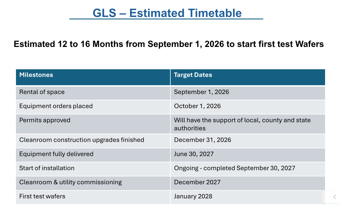

At age 75, Dr. Richard Thurston, former General Counsel of TSMC, is returning to the entrepreneurial arena with the launch of Great Lakes Semiconductor to solve a structural blind spot in the global chip ecosystem. Inspired by decades of working alongside industry titans Morris Chang and Jack Kilby, Thurston aims to democratize innovation and revive the grassroots hardware startup culture that initially fueled the fabless revolution.
Solving the “Missing Middle”
In the latest TechSoda podcast, Thurston points to a widening gap in the supply chain: the “missing middle.” In its early years, TSMC actively nurtured emerging fabless startups—including Nvidia, Qualcomm, and Broadcom—by running experimental prototypes and low-volume “hot lots.” However, as foundries scaled into massive mega-fabs focused on delivering millions of units, capacity became too tight to accommodate small-batch trial runs.
This dynamic has locked out small and medium enterprises (SMEs), university researchers, and startups from accessing shuttle runs and wafer tape-outs, causing venture capital for early-stage hardware to stall.
A Modular Blueprint for Prototyping
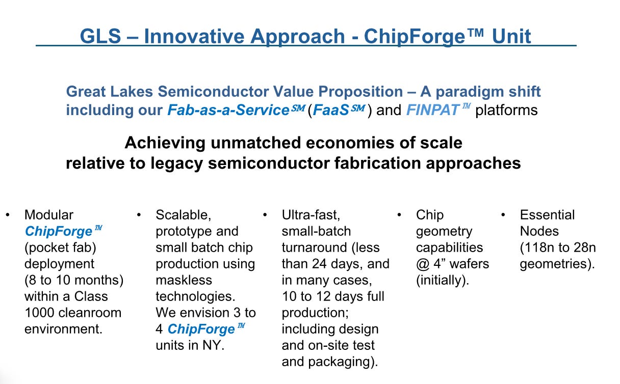
Drawing on a concept proposed by microchip co-inventor Jack Kilby in the 1980s—fitting a production line into a modular container—Great Lakes Semiconductor is building low-cost, decentralized mini-fabs designed for rapid iteration rather than mass manufacturing:
Modular Fabrication: Self-contained units operating in Class 1,000 cleanrooms with single-wafer processing on 4-inch wafers.
Agile Tooling: Utilization of electron-beam (eBeam) lithography instead of multi-million-dollar EUV machinery, optimizing turnaround times for mature and legacy nodes.
Integrated Backend: On-site 3D heterogeneous packaging combined with AI-driven predictive supply-chain intelligence.
“An Innovation Funnel” for Foundry Giants: Mini-fabs are designed to complement, not compete with, high-volume manufacturers. By handling early validation on agile 4-inch wafers and direct-write eBeam systems, the model absorbs early-stage development risk before funneling qualified designs to certain foundries for volume scaling.

Strategic Value for Taiwan
Rather than competing with foundry giants, Great Lakes Semiconductor is structured to serve as an upstream “innovation funnel” for Taiwan’s semiconductor ecosystem:
Volume Production Pipeline: The venture acts as an external incubator, developing and testing mature designs before porting them over to collaborative partners for high-volume commercial scaling.
Supply Chain Diversification: Taiwanese specialty chemical, gas, and water infrastructure providers gain opportunities to supply a new decentralized mini-fab footprint expanding across North America and Europe.
R&D & Packaging Alliances: Deepening ties with Taiwanese institutions like ITRI and domestic memory makers allows Taiwan to capture emerging opportunities in physical AI, specialized sensors, and heterogeneous integration without diverting advanced capacity from core high-volume lines.
Investor & Funding Status
Private Capital & Venture Backing: The venture is actively seeking additional equity investors and strategic commercial partners to fund broader expansion.
Government Grants & Subsidies: The company is working with regional economic development authorities for direct grants and site-development funding to offset capital expenditures.
Foundation & Ecosystem Financing: Thurston is collaborating with Paul Hsu (Xu Xiaobo)—founder of Epoch Foundation—to explore foundation-based funding models focused on R&D support and intellectual property development.
Government Engagement & Country Participation
While formal multilateral commitments have not been fully finalized, Great Lakes Semiconductor is in active discussions with 7 key countries and government bodies:
India: Direct discussions with the India Semiconductor Mission (ISM) regarding deploying the ecosystem within India.
United States: State and municipal leadership are actively competing for installations, including direct engagement from the governors of Texas and Idaho, as well as the mayors of Cleveland and Detroit.
Taiwan: Discussions with various public and private organizations, such as ITRI (Industrial Technology Research Institute), logic, III-V, MEMS, and memory foundries.
Ireland & Vietnam: Active bilateral talks to assess local deployment feasibility.
Canada & Germany: Targeted for cross-border North American integration and European expansion including the Ferroelectric Memory Company of Germany, with which GLS has recently executed a non-binding LOI.
Japan: Strategic supply-chain alignment through seven core toolmakers (e.g., Daikin, Disco) and engineering teams.
Planned Mini-Fab & Lab Locations
Thurston aims to scale the modular footprint to around 10 U.S. locations and 6 to 10 international sites over the next five years:
North American Sites:
Fishkill, New York: Advanced 3D packaging and back-end integration center in partnership with APES.
Cleveland & Detroit: Repurposing existing industrial infrastructure and warehouses into modular cleanrooms.
Texas & Idaho: Sites under discussion with state economic leadership.
Canada: Facilities planned along the broader Great Lakes cross-border manufacturing corridor.
Global Target Locations:
Taiwan, Japan, India, Ireland, Germany, and Vietnam.
Several takeaways from the interview:
· Reviving the Hardware Startup Engine: As the foundry industry scaled toward multi-billion-dollar gigafabs, it created a “missing middle” that crowded out early-stage prototypes and university R&D. Low-cost modular mini-fabs provide an accessible path to reignite hardware venture creation and rapid iteration.
· An Innovation Funnel for Foundry Giants: Mini-fabs are designed to complement, not compete with, high-volume manufacturers. By handling early validation on agile 4-inch wafers and direct-write eBeam systems, the model absorbs early-stage development risk before funneling qualified designs to TSMC for volume scaling.
Untapped Value in Mature Nodes & Heterogeneous Packaging: Innovation in the semiconductor sector extends far beyond sub-3nm logic. Significant market growth lies in legacy nodes, specialized sensors for robotics and physical AI, and advanced 3D packaging that integrates disparate chipsets efficiently.
The Need for Sustainable, Long-Term Industrial Policy: Short-term subsidies and narrow defense-focused grants are insufficient to sustain a thriving chip industry. Sustainable ecosystems require continuous, multi-generational funding and open international talent exchange similar to models established in Taiwan, Singapore, and Japan.
Democratizing the Global Chip Footprint: By replacing monolithic cleanrooms with modular equipment inside standard Class 1,000 spaces, chipmaking can expand into existing industrial sites and warehouses globally, lowering entry barriers for regions outside traditional semiconductor hubs.