

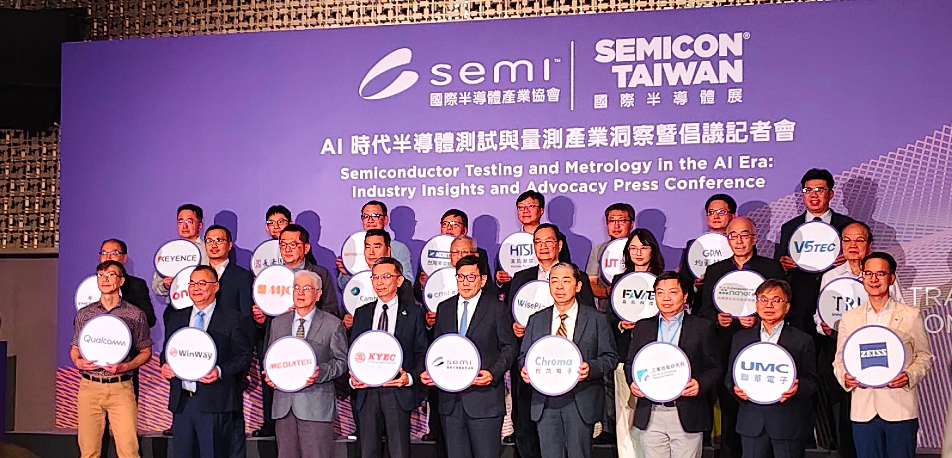
At a dedicated SEMI press conference highlighting the growing importance of semiconductor testing and metrology technologies in the AI era, industry leaders—including SEMI Global Chief Marketing Officer Terry Tsao, Chroma ATE Inc. CEO I-Shih Tseng, and KYEC President Gauss Chang—shared valuable insights drawn from decades of industry experience, while offering their perspectives on the technologies and innovations shaping the industry’s future.
In the prevailing narrative of the artificial intelligence boom, the spotlight rarely shifts from massive wafer foundries, superstar chip architects, and pristine cleanrooms. Yet, insights shared by the aforementioned semiconductor industry leaders reveal a profound inversion across the supply chain: testing and metrology have transformed from an overlooked back-end cost center into the most critical, high-stakes battleground of the AI hardware ecosystem.
As chipmaking moves from planar silicon to complex heterogeneous architectures, the industry faces an unyielding reality: if cutting-edge silicon cannot be physically measured and verified in real time, it cannot be deployed.
The Past: The Forgiving “Three-No” Consumer Era
To understand why metrology is suddenly taking center stage, one must examine why it was marginalized for decades. During the peak of consumer electronics, semiconductors were predominantly low-cost, single-die components destined for basic mobile phones, digital cameras, and MP3 players.
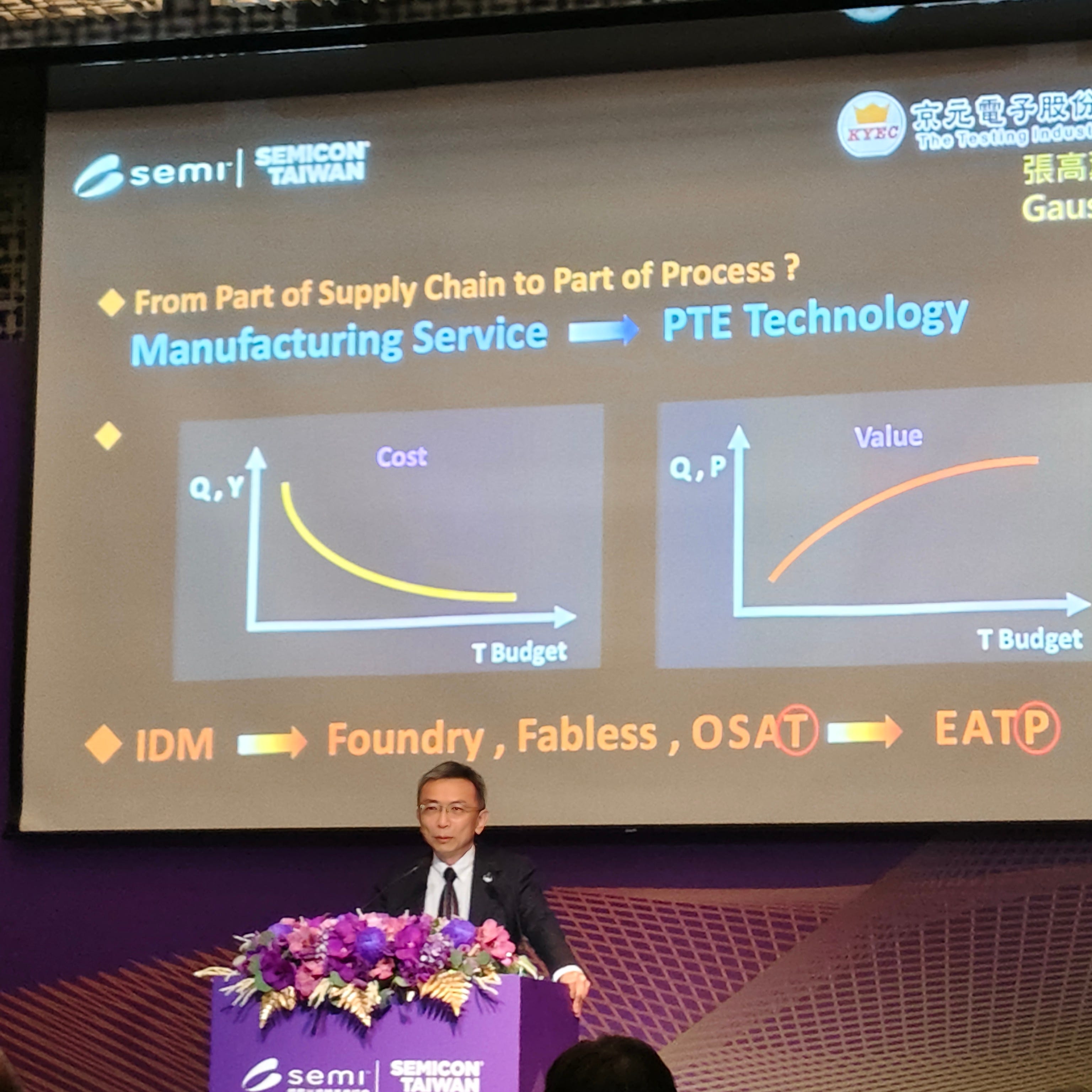
“Historically, the consumer era operated on a ‘three-no policy’: no return, no replenishment, and no exchange,” noted Gauss Chang, President of King Yuan Electronics Corp. (KYEC).
In the past, individual silicon units for consumer electronics cost pennies to manufacture, the financial risk of a single component failing in the field was negligible. Manufacturers routinely compensated for defect rates by throwing an extra 3% buffer of free chips into every shipping batch. Within this economic model, testing was viewed as a necessary evil—a non-value-added bottleneck where operational budgets were aggressively squeezed and machine test times were minimized to keep assembly lines moving.
The Present: The Astronomical Cost of AI Failure
The AI revolution has dismantled this disposable mindset. Modern high-performance computing platforms are no longer single flat chips laid out side-by-side like suburban homes. Instead, they are dense, interconnected metropolises built via advanced 3D packaging technologies such as Chip-on-Wafer-on-Substrate (CoWoS), System-on-Integrated-Chips (SoIC), and High Bandwidth Memory (HBM) stacks.
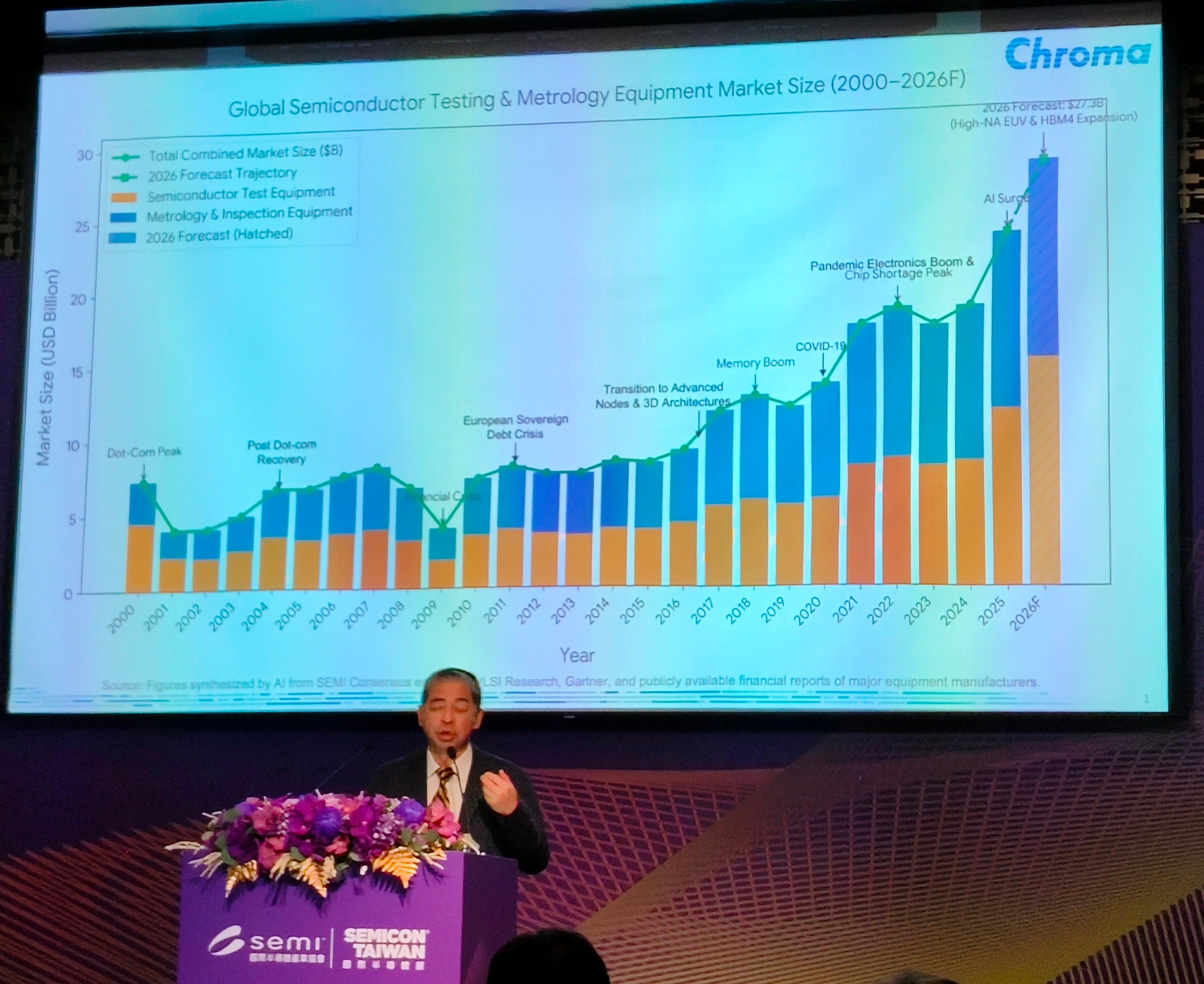
In these heterogeneous systems, individual silicon units carry astronomical valuations. More critically, once multiple chiplets and memory dies are vertically integrated into a single package, traditional physical probing becomes impossible. A single microscopic defect buried deep within an unprobed 3D stack will destroy the entire package, turning a multi-million-dollar AI server rack into an expensive paperweight.
“AI products integrate advanced packaging, high-bandwidth memory, optical components, and high-power computing into heterogeneous stacks. In this cost-high-value landscape, the industry demands zero tolerance, zero impact,” emphasized I-Shih Tseng, CEO of Chroma ATE.
The shift is equivalent to moving from inspecting mass-produced plastic toys—where a defect is simply tossed into a bin—to inspecting the single microscopic engine of a spacecraft mid-flight while it burns at maximum capacity.
Front-Loading R&D: Testing Before Technology Matures
Because the cost of failure is catastrophic, the industry can no longer afford to treat testing as a gatekeeper checking homework at the end of the manufacturing line. Today, product architectures are designed years ahead of manufacturing process maturity, forcing metrology to move directly into the initial research and development phase.
Testing parameters now act as the primary feedback loop defining what is physically possible to fabricate. This shift toward early co-development is demonstrated by KYEC’s strategic alliance with Nvidia, established in the fourth quarter of 2005 to test parallel computing architectures. Through the EATP (Equipment, Accessory, Test, and Product) framework, test engineers build software emulations and specialized test hardware alongside chip architects, calibrating measurement instruments years before volume manufacturing begins.
New Frontiers: Multi-Physics and Robotic Vision
Driven by escalating architectural complexity, the global semiconductor equipment market is projected to reach $230 billion by 2028, with testing equipment expanding rapidly from $17.7 billion in 2025 to $20.8 billion by 2028. This capital surge is propelled by two unprecedented physical frontiers:
Silicon Photonics and Co-Packaged Optics (CPO): Replacing traditional copper electrical interconnects with light requires testing optical lasers and waveguides embedded directly inside 3D compute stacks. Metrology tools must execute dynamic multi-physics testing—measuring optical alignment, light intensity, electrical signaling, and thermal warping simultaneously. If heat-induced expansion causes a component to misalign by a fraction of a hair, the optical signal collapses.
Physical AI and Machine Vision: Moving AI into autonomous robotics requires testing CMOS Image Sensors (CIS)—such as those developed in partnerships between TSMC and Sony—not for human photographic aesthetics, but for ultra-high-velocity data fidelity under unpredictable real-world environments.
Systemic Bottlenecks Demanding Prioritized Investment
Despite robust commercial expansion, industry executives warn that severe structural roadblocks could choke the AI hardware pipeline unless metrology is prioritized across academic, financial, and institutional agendas:
The Cross-Disciplinary Talent Chasm: Traditional university curricula isolate electrical engineering and optical physics. Terry Tsao, SEMI Global Marketing Officer and President of SEMI Taiwan, highlighted an acute shortage of systems-level engineers proficient in both domains, prompting SEMI to lobby for specialized optical-electrical university programs.
Breaking the “Affiliation Trap”: I-Shih Tseng warned that metrology R&D has historically been subordinated as a minor line item inside broader wafer fab budgets. Foundational breakthroughs require standalone funding for basic sciences, pure mathematics, and advanced material research rather than incremental tool tweaks.
Parts-Per-Billion (PPB) Verification Hurdles: Defect rates in heterogeneous silicon are now measured in parts per billion—analogous to locating a single contaminated drop of water in an Olympic-sized swimming pool. To alleviate the immense capital cost of validating new test methodologies on active production lines, SEMI is advocating for shared, government-backed advanced testing platforms.
Transitioning to Global Standard-Setters: Manufacturing and packaging hubs like Taiwan cannot remain solely execution powerhouses. Setting global measurement standards for emerging technologies like CPO is vital to authoring the industry’s technological trajectory rather than reacting to external rules.
Elevating testing and metrology into an independent, well-funded R&D pillar is no longer an optional optimization. It is the foundational requirement upon which the scalability, reliability, and physical realization of the AI era depend.
Editor’s note: The podcast and the notes were created in collaboration with NotebookLM and Gemini. The author covered the press conference in person and is responsible for the final editorial judgement.


