
IP Insight #3: TSMC Accelerates in Silicon Photonics While Intel Becomes More Selective
Two Different Strategic Realities Behind the Patent Trends
When silicon photonics was discussed over the past decade, the company most often associated with it was Intel. That association is beginning to shift.
Recent patent data in the United States suggests a divergence in activity. TSMC has increased its filings in core silicon photonics technologies over the past two years, while Intel’s annual filings in this area have declined.
Patent counts do not equate to technical superiority. However, they do provide insight into where companies are allocating capital, engineering resources, and long-term strategic focus. In that sense, the divergence is meaningful.
The contrast reflects two very different business realities. On one side is a foundry responding to accelerating AI customer roadmaps. On the other is a large IDM navigating capital intensity, process node catch-up, product competition, and structural transformation.
Silicon Photonics as an AI Era Bottleneck Solution
Silicon photonics integrates optical components directly into silicon chips or advanced packaging, enabling data transmission via light instead of electrical copper interconnects.
In the AI era, this capability is becoming increasingly important.
As GPU, TPU, and accelerator performance continue to scale, bottlenecks are shifting away from raw compute. Instead, interconnect bandwidth and power efficiency between chips and between racks inside data centers are emerging as critical constraints.
This is where CPO (co-packaged optics) and optical I O architectures enter the discussion. By embedding optical engines closer to compute silicon, electrical path lengths are reduced, signal conversion losses are minimized, and higher bandwidth can be achieved at lower power consumption.
Intel has been an early and credible participant in silicon photonics, integrating optical technologies into server and networking applications and demonstrating multiple proof-of-concept systems.
However, since 2023, patent activity suggests a shift in intensity.
The Patent Divergence
Industry analyses of US-based silicon photonics patents indicate that TSMC and Intel were closely matched as recently as 2023.
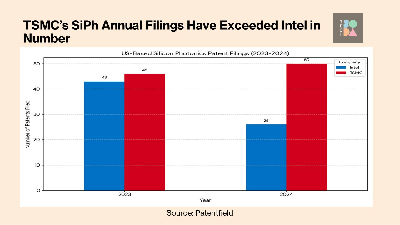
In 2023,
TSMC filed approximately 46 relevant patents
Intel filed approximately 43
In 2024
TSMC increased to roughly 50
Intel declined to about 26
The magnitude of this change suggests a shift in allocation rather than a statistical fluctuation.
This trend is consistent with a broader recalibration at Intel. Between 2015 and 2020, Intel expanded patent filings aggressively across multiple technology domains. Since 2023, overall filings have moderated, particularly in certain frontier areas.
Silicon photonics appears to be part of that broader shift toward selectivity. In other words, the divergence is less about photonics itself and more about capital allocation under different business models.
Why TSMC Is Increasing Activity
AI Customer Roadmaps Are Driving Integration Requirements
Large language models (LLMs) and AI training clusters are pushing data center architectures to new scales. Compute can scale by adding more GPUs. Memory capacity can scale through HBM stacking. But interconnects between GPUs and between racks become increasingly constrained by power and bandwidth when relying solely on copper-based architectures.
CPO and silicon photonics provide a potential pathway to address these constraints.
For TSMC, this is not a speculative research topic. Major customers such as NVIDIA and AMD are designing future architectures that depend heavily on advanced packaging integration.
Optical I O is increasingly discussed within those roadmaps.
From a foundry perspective, enabling that integration strengthens platform relevance.
From Demonstration to Production Alignment
Reports indicate that TSMC intends to integrate silicon photonics solutions into advanced packaging platforms such as CoWoS and SoIC, targeting 1.6T optical module generations around 2025 and broader scaling thereafter.
This alignment with production timelines is important. It signals integration into customer roadmaps rather than isolated demonstration efforts.
Architectures such as COUPE, Compact Universal Photonic Engine, illustrate this approach. Public descriptions suggest a three-layer stack combining a 6nm electronic die, a 65nm photonic die, and an intermediate integration layer designed to support both horizontal and vertical optical connectivity.
The emphasis appears to be on modular reuse across multiple customer programs rather than one-off custom designs.
In this context, patent filings function as protective infrastructure around a production-oriented platform strategy.
Platform Differentiation in the Foundry Model
Unlike an IDM that sells end products, a pure play foundry competes on process technology and integration capability.
TSMC’s patent focus in silicon photonics appears concentrated in areas such as:
Integration within 300mm CMOS manufacturing, advanced packaging integration of GPU, HBM, and optical engines, thermal management, TSV structures, passive alignment, and material reliability.
If these integration methods are protected, customers designing large-scale AI packages may face higher switching costs.
From a strategy perspective, silicon photonics strengthens platform stickiness for a foundry that directly supports long-term wafer and advanced packaging revenue.
Why Intel’s Activity Appears More Selective
Intel remains a significant technology holder in silicon photonics. The moderation in filings should not be interpreted as abandonment.
However, Intel is simultaneously investing in advanced nodes such as 18A, expanding fabrication capacity in the United States and Europe, defending CPU and accelerator competitiveness, and building out its foundry services business.
Capital expenditure requirements are substantial. R&D prioritization becomes unavoidable. In that environment, patent strategy tends to become more focused on areas with clearer near-to-mid-term revenue linkage. Intel has also adjusted certain optical communications activities. For example, transceiver-related assets were transferred to Jabil, reflecting the refinement of product focus.
In advanced packaging discussions, licensing and ecosystem approaches are increasingly emphasized alongside internal deployment. Rather than broad expansion, the pattern suggests protection of core IP while narrowing the scope of new filings. From a strategic standpoint, silicon photonics may currently occupy a medium to long-term option position within Intel’s broader portfolio, rather than a near-term growth driver.
Two Strategic Realities on the Same Track
The contrast is not simply about who believes in silicon photonics more. For TSMC, silicon photonics can extend an already dominant advanced packaging platform. AI customers are actively scaling orders for leading-edge process nodes and 3D integration. Optical integration represents a logical extension of that trajectory.
For Intel, the strategic landscape is more complex. Process leadership recovery, product competitiveness, fab construction, and foundry expansion all compete for capital and management focus.
Under those conditions, even important technologies may advance at a measured pace.
What Patent Counts Do and Do Not Tell Us
Patent volumes function as indicators of strategic emphasis, not definitive measures of technical leadership or commercial outcome. In silicon photonics, the more relevant questions are structural: Are these filings reinforcing a manufacturing and packaging platform that customers will build around for the next decade? Or are they consolidating a defensible intellectual property position that preserves long-term strategic leverage?
TSMC’s recent activity suggests an effort to deepen platform stickiness, extending its advanced packaging ecosystem into optical integration and embedding itself more tightly into AI customer roadmaps.
Intel’s recent pattern suggests a different emphasis: protecting core architectural and integration IPs while managing capital discipline across multiple strategic priorities.
One strategy compounds platform dependency. The other builds an intellectual property arsenal.
Same technology. Two strategic games.
How those two approaches ultimately reshape bargaining power within the AI supply chain remains an open question — and one that will define the next phase of competition in silicon photonics.
In the next article (IP Insight #4), we take a further deep dive into the portfolios and what they tell us about the two semiconductor giants’ strategies.

About the author:
Editor’s Note: The IP Insights Series is a collaborative initiative between Deeli AI, Mission International Patent & Trademark Office, and TechSoda, powered by the Deeli AI platform to analyze patents and papers.
Previous IP Insight articles:


 | A guest post by
|