
Executive Summary: The “System-Level Foundry” Shift
Understanding TSMC’s current Intellectual Property (IP) layout is critical because it reveals a fundamental transformation: TSMC is no longer just shrinking transistors; it is architecting an integrated AI infrastructure. By cross-referencing recent patent filings with the January 15th earnings call, three strategic imperatives emerge:
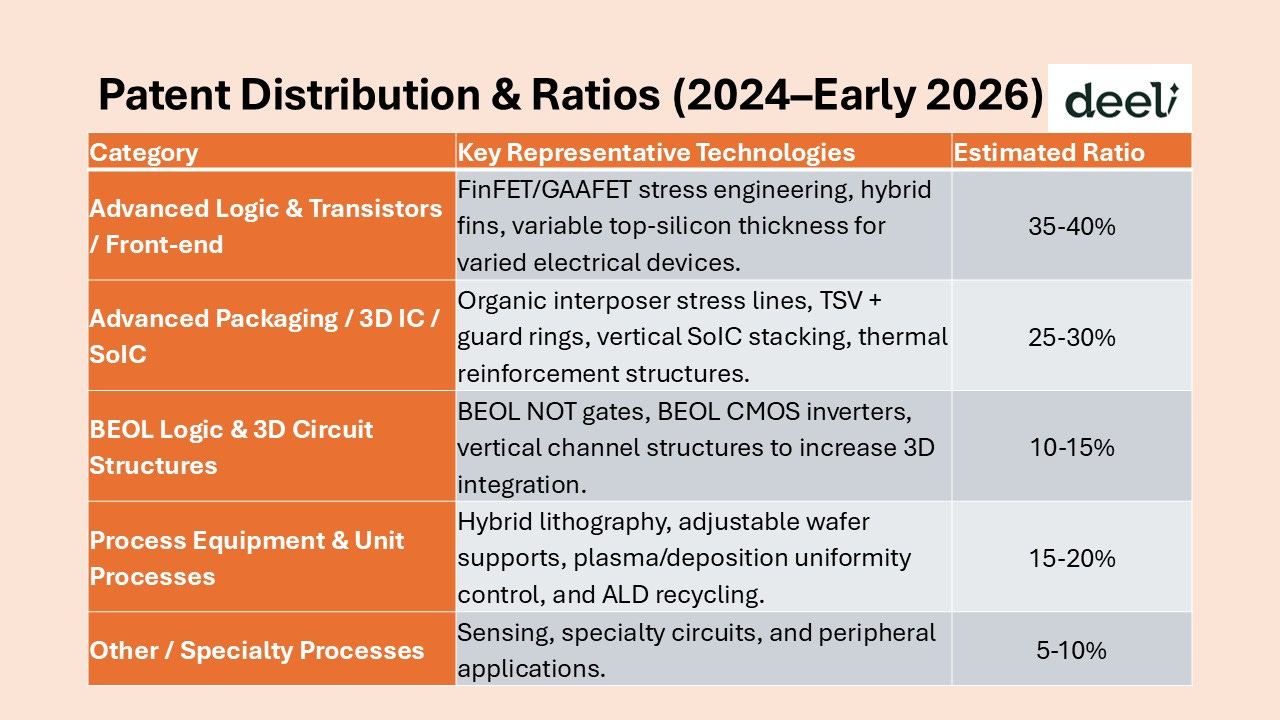
Breaking the Memory/Power Wall: The pivot toward BEOL (Back-End-Of-Line) interconnect innovation, BEOL compatible logic devices, and 3D IC structures (roughly 25–30% of the patents in our sample) indicates that TSMC increasingly views “interconnect and thermal management,” rather than front-end node scaling alone, as the key bottleneck to be addressed over the coming decade.
Packaging as a Primary Moat: By elevating CoWoS and SoIC as a second strategic battleground alongside advanced wafer fabrication, TSMC is leveraging technical complexity and tight integration to lock in high-value AI customers such as NVIDIA and AMD, and to raise the competitive bar for alternative foundries and OSATs.
Financial Fortification: A growing portfolio of patents around equipment design and process control effectively reinforces TSMC’s cost and yield position, supporting its ambition to sustain around 60% plus gross margins even as overseas fabs and the N2 ramp introduce 2–4 percentage points of structural margin dilution.
1. AI/HPC Growth Driving Surge in Advanced Node + 3D Structure Patents
Earnings Call Summary: Management explicitly stated that the revenue CAGR for AI accelerators will approach 55% from 2025–2029. The HPC platform already accounts for over half of total revenue and will continue to grow.
Patent Trends: In the past two years, a massive number of patents have been filed in fin structure stress engineering (designing and tuning stress in FinFET channels and layouts), hybrid fins, BEOL compatible logic, and TSV plus guard rings. These are designed to maintain high performance, high signal integrity, low power, and 3D‑stackable logic foundations beyond the N3/N2 nodes.
Insight: TSMC views AI growth as “structural and long-term.”
Instead of simple line-width shrinking, resources are being poured into architectures like GAAFET, BEOL logic, and 3D-IC that can sustain growth for a decade. This grants TSMC significant leverage in architectural flexibility and 3D integration for future generations (N2P, A16).
2. AI Capacity Tightness → Significant Increase in Packaging/Thermal Patents
●Earnings Call Summary: Management repeatedly emphasized that AI-related capacity is “extremely tight.” Capital expenditure (Capex) has been raised significantly, with a large portion dedicated to expanding advanced packaging and AI-specific packaging capacity.
● Patent Reflections:
o Stress Management: Stress-release lines and reinforcement structures within silicon or organic interposers/substrates to solve mechanical reliability issues in multi-chip packaging.
o Mechanical Strength: In Fan-out/SoIC packaging, specific die arrangements and molding/cutting designs are used to improve mechanical integrity.
o Active Cooling: Integration of thermal modules with cavities and embedded TECs (Thermoelectric Coolers) directly atop heterogeneous packages to address active cooling for high-power AI chiplets.
Insight: For AI GPUs/ASICs, the bottleneck is no longer just the transistor, but “I/O Bandwidth + Heat Dissipation + Mechanical Reliability.” TSMC’s patents show they aren’t just building more CoWoS lines; they are turning packaging, thermal modules, and mechanical design into a combined “technical moat.” This aligns with the high CapEx allocated to AI advanced packaging.
3. High Capex & Gross Margin Goals → Equipment/Process Control Patents are Key
● Earnings Call Summary: TSMC set a 2026 gross margin target of 63–65%, with a long-term goal of remaining above 56% throughout cycles, despite the 2-4 percentage point dilution from the initial N2 ramp-up and overseas fab costs.
● Patent Trends: Significant investment in “Process Efficiency and Uniformity”:
o Hybrid Lithography Systems: Combining traditional reduction exposure with direct-beam writing to optimize different regional densities, increasing throughput and lowering costs without sacrificing critical pattern quality.
o Tunable PEZ (Plasma Exclusion Zone): Using adjustable rings to control plasma distribution, improving uniformity between the wafer edge and center, which directly impacts yield.
o Highly Adjustable Wafer Supports/Chucks: Fine-tuning the distance between the wafer and the process head to ensure more stable deposition/etching/exposure conditions, thereby reducing defects.
o ALD Precursor Recycling & Detection: Systems to increase material utilization and lower the unit cost per process step.
Insight: To defend high margins amidst massive Capex and the costs of overseas expansion/N2 ramp-up, TSMC relies on more than just pricing. They use “Equipment and Process Control” patents to push the cost and yield of every single wafer to the limit, echoing management’s confidence in their margin targets.
4. N3/N2/N2P Roadmap → Extending into BEOL/3D/Thermal Management
● Earnings Call Highlights:
o N3 gross margin will exceed the corporate average within 2026, becoming the mainstay for AI/HPC.
o N2 mass production has begun; N2P and A16 are on the way, emphasizing new architectures such as backside power delivery networks for logic.
● Patent Presentation:
o BEOL Logic: Implementing BEOL‑compatible logic elements together with specialized interconnect structures in the BEOL stack, enabling additional logic capacity above the FEOL and supporting finer-grained 3D partitioning
o TSV Optimization: Improving guard rings and metal layouts around TSVs to reduce parasitic effects and noise coupling, clearly preparing for higher signal integrity in 3D chip stacking.
o Thermal Paths: Designs for internal thermal paths using tailored cavities, high-conductivity materials, TEC integration, and mechanical stress reinforcement to handle the thermal limits of high-power-density AI chips.
Insight: TSMC does not view “N2 → A16” as just a nanometer figure. It is an entire platform combining BEOL-compatible logic, 3D-IC, advanced packaging, and co-designed thermal management solutions. Future product differentiation will depend on total system performance, performance per watt, and bandwidth, rather than just the nominal logic node.
Strategic Inferences
Packaging as the “Second Main Battlefield”
With Capex reaching $52–56 billion in 2026 (10-20% for packaging/testing/mask) and CoWoS capacity doubling to 125k–130k wafers/month by late 2026, TSMC is elevating advanced packaging from a “back-end support role” to a strategic level equal to wafer fabrication. The goal is to use CoWoS/SoIC/InFO combined with HBM/Chiplets as the solution to AI/HPC bottlenecks.
Global Capacity: Overseas Fabs Bound to High-End Packaging
TSMC isn’t just building wafer fabs in Arizona; they are planning CoWoS/SoIC packaging lines there (2026–2029) to serve products like NVIDIA Rubin and AMD MI400. Overseas expansion is not just “capacity replication” but a “High-End Logic + High-End Packaging” pair, allowing for the full AI GPU/ASIC flow to be completed locally.
Conclusion
TSMC is upgrading its positioning from a “leader in advanced process nodes” to a “critical infrastructure provider for the AI/HPC era.”
1. Long-term Structural Demand: Focused investment in N2/N2P/A16 and 3D/BEOL structures targets a decade of AI demand.
2. System-Level Moat: Shifting competition from single-node advantages to “Integrated System Platforms” (Logic + 3D + Packaging + Thermal).
3. Financial Resilience: Using equipment and process control patents to create a “cost and yield moat” that maintains ~60% gross margins and high ROE.
Editor’s Note: The IP Insights Series is a collaborative initiative between Deeli AI, Mission International Patent & Trademark Office, and TechSoda.
