
TSMC Announces A14 Process at North America Technology Symposium
Next-Generation Process Technology Targeting Production in 2028
Next-Generation Process Technology: A14 Node
TSMC officially unveiled its A14 process technology, targeting production in 2028. A14 is based on the company’s second-generation GAAFET (Gate-All-Around Field-Effect Transistor) nanosheet transistors and introduces the new NanoFlex™ Pro standard cell architecture.
A14 is positioned to deliver a 15% performance boost at the same power consumption as N2 (TSMC’s 2nm node entering production this year), or 30% lower power at the same speed. Additionally, it offers a 20% increase in logic density compared to N2.
The NanoFlex™ Pro architecture enables greater design flexibility, allowing chip designers to fine-tune transistor configurations for optimal power, performance, and area (PPA) for specific workloads.
Design-Technology Co-Optimization (DTCO) and NanoFlex™ Pro
TSMC continues to leverage DTCO, evolving its NanoFlex™ standard cell architecture to NanoFlex™ Pro. This approach enhances performance, power efficiency, and design flexibility, supporting the development of highly customized and efficient chips for diverse applications.
While detailed technical differences between NanoFlex and NanoFlex Pro were not disclosed, NanoFlex Pro is expected to provide more granular control and better software tools for optimizing transistor-level trade-offs.
Advanced Packaging and 3D Integration
TSMC showcased advancements in packaging technologies, crucial for AI and high-performance computing (HPC):
CoWoS® (Chip on Wafer on Substrate): Plans for 9.5 reticle size CoWoS in 2027, enabling integration of 12 or more HBM (High-Bandwidth Memory) stacks with leading-edge logic in a single package.
System-on-Wafer-X (SoW-X): A new CoWoS-based offering that creates wafer-sized systems with computing power 40 times greater than current CoWoS solutions, scheduled for volume production in 2027.
Silicon Photonics: Introduction of the Compact Universal Photonic Engine (COUPE™) to enhance data transfer rates by integrating silicon photonics with N12 and N3 logic.
Segment-Specific Innovations
High Performance Computing (HPC): New packaging and integration technologies to meet AI’s demand for more logic and memory bandwidth, including integrated voltage regulators for improved power delivery.
Smartphones: Introduction of N4C RF technology, offering 30% power and area reduction over N6RF+, supporting next-gen wireless standards like WiFi 8 and AI-rich edge devices. Risk production is expected in Q1 2026.
Automotive: N3A process is entering production for automotive applications, meeting stringent quality and reliability standards for ADAS and autonomous vehicles.
Internet of Things (IoT): Ultra-low power N6e process is now in production, with N4e targeting further power efficiency improvements for edge AI applications.
Strategic Position and Roadmap
TSMC’s roadmap maintains its leadership in logic scaling and platform innovation, with A14 and subsequent nodes (such as A16) pushing beyond the 2nm threshold.
The company is expanding manufacturing capacity, including plans for new factories in Arizona, and is preparing for high-volume production of advanced nodes both in Taiwan and the US.
TSMC’s suite of interconnected technologies is designed to support innovation across cloud, edge, automotive, and IoT markets, reinforcing its role as a critical enabler for AI and next-generation computing.
Industry and Customer Engagement
The North America Technology Symposium, TSMC’s flagship customer event, highlighted these advancements to over 2,500 attendees, including opportunities for startups to showcase innovations and connect with investors.
Summary Table: TSMC A14 Node vs. N2 Node
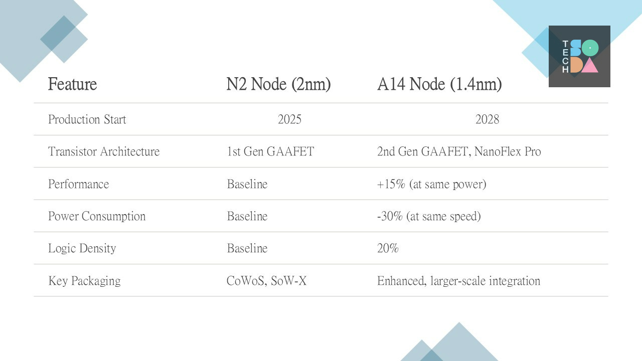
FeatureN2 Node (2nm)A14 Node (1.4nm)Production Start20252028Transistor Architecture1st Gen GAAFET2nd Gen GAAFET, NanoFlex ProPerformanceBaseline+15% (at same power)Power EfficiencyBaseline-30% (at same speed)Logic DensityBaseline+20%Key PackagingCoWoS, SoW-XEnhanced, larger-scale integration
TSMC’s latest announcements underscore its commitment to advancing semiconductor technology for AI, HPC, mobile, automotive, and IoT applications, with a focus on performance, power efficiency, and design flexibility through innovations in both process technology and advanced packaging.