


TSMC 2025 Taiwan Technology Symposium Reveals Roadmap Toward AI-Driven, Energy-Efficient Future
TSMC (台積電) unveiled a sweeping vision for the future of semiconductors at its 2025 Taiwan Technology Symposium in Hsinchu, spotlighting transformative advancements across process technology, AI applications, packaging, and power management. With artificial intelligence reshaping industry landscapes, the world’s largest foundry positioned itself as a central enabler of this revolution.
AI as the Next Frontier: From Generative to Physical
TSMC Asia-Pacific business director Rui-yang Wan (萬睿洋) identified "Physical AI"—including humanoid robots and autonomous vehicles—as the next major wave following generative and agent-based AI. He projected that the global AI robot market value will exceed US$35 billion in 2030, and by 2030, one in ten cars will be autonomous.
Wan cited 2024 as a breakthrough year for AI, with Nobel Prizes awarded for innovations in machine learning and protein structure prediction. He emphasized AI's accelerating impact in fields ranging from cancer diagnostics to astronomy and geophysics.
Looking ahead, generative AI is expected to transform over 40% of daily work tasks by 2028, while agent-based AI could handle 15% of decision-making, including travel planning and personal scheduling.
TSMC forecasts a proliferation of physical AI with 1.3 billion AI robots globally by 2035, expanding to 4 billion by 2050—including 650 million humanoid robots. This trend will push AI from the cloud to the edge, requiring breakthroughs in chip performance, power efficiency, and miniaturization.
Technological Milestones: A14, A16, and 2nm Advances
TSMC Co-COO Kevin Zhang (張曉強) outlined a roadmap of new process nodes:
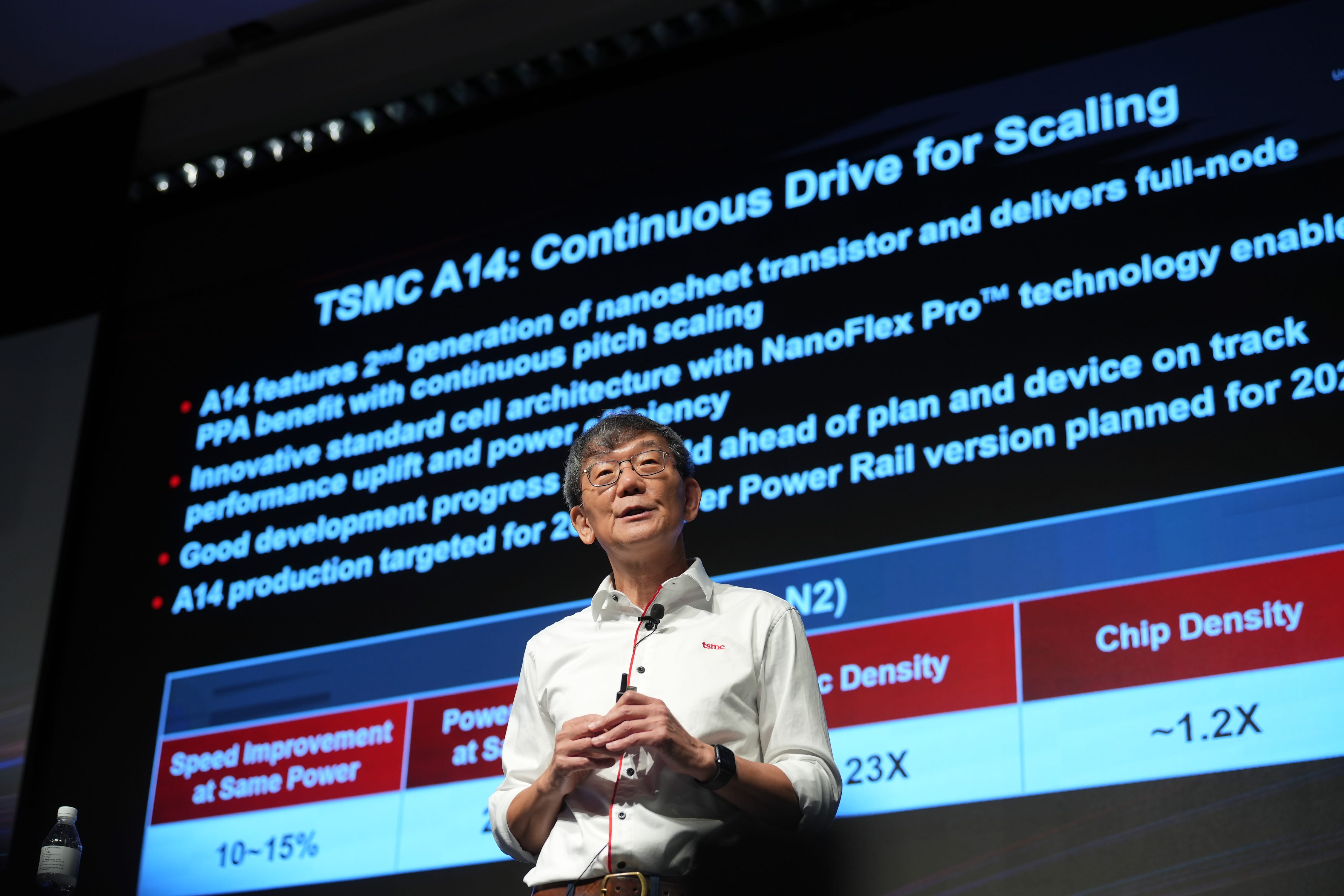
A14 (1.4nm): Planned for mass production in 2028, A14 will offer a 15% speed boost, 30% power reduction, and 20% greater logic density compared to N2. It introduces “NanoFlex Pro” for better performance and flexibility, and a version with Super Power Rail (SPR) backside power delivery is due in 2029.
A16 (1.6nm): Tailored for data center AI and HPC, A16 with SPR will begin volume production in late 2026.
N2 (2nm): Mass production starts in late 2025. Its initial adoption by AI customers is already double that of N5 in its first year.
N3 (3nm): Now in its third year, N3’s capacity will grow 60% in 2025, with derivatives like N3E, N3P, and N3X supporting diverse needs from HPC to automotive chips.
Packaging and Integration: 3DFabric, SoW-X, and Beyond
TSMC detailed major packaging advances:
SoIC (System on Integrated Chips) for 3D silicon stacking will enter volume production in 2025 for N3-on-N4 configurations.
CoWoS (Chip-on-Wafer-on-Substrate): CoWoS-L with a 5.5x mask size launches in 2026; CoWoS with a record 9.5x mask size, integrating 12+ HBM stacks, is planned for 2027.
SoW-X (System-on-Wafer): Offering 40x performance improvement over CoWoS, it mimics full server rack capabilities and is set for 2027 mass production.
Foundry Expansion and Regional Growth
TSMC announced plans to build 9 new fabs in 2025 alone—8 wafer fabs and 1 advanced packaging plant. Of these, 11 fabs are currently under construction in Taiwan across Hsinchu, Tainan, Taichung, and Kaohsiung.
Notably, Fab 25 in Taichung will begin construction by year-end and aims for 2028 production using technology beyond 2nm.
In 2024, TSMC's Asia-Pacific clients used over 1.8 million wafers for 2,400+ products, contributing 10% of revenue, with 300 new products entering mass production soon.
Sustainability and Energy Challenges
A central issue raised at the forum was AI's exploding power demands. Delta Electronics’ Power Systems General Manager, Chen Ying-Yuan (陳盈源), revealed AI chips now consume up to 1,200W—tripling in four years—with projections reaching 2,400W by 2026. A single server rack with 576 GPUs could consume 1 Megawatt, matching 10,000 homes.
Delta outlined six infrastructure innovations, including:
Power Conditioning Systems (PCS) to flatten AI load spikes
Liquid cooling systems using two-phase metal chambers
Micro and containerized data centers for rapid deployment
High-frequency power modules to shrink transformer sizes by 90%
Delta is proposing solutions like PCS (Power Conditioning System) dynamic load compensation modules, high-frequency power conversion modules, and Two-Phase Metal Chamber cooling technology to address these challenges.
Next-Gen Special Technologies
TSMC is also pushing forward in niche domains:
Memory: RRAM (12nm certified for automotive) and MRAM (22nm in production, 16nm ready, 12nm in development).
IoT & RF: N4C RF cuts power and area by 30% vs. N6RF+, supporting Wi-Fi 8 and advanced TWS audio. Expected in trial production by Q1 2026.
Displays: 16HV FinFET platform for foldable OLED and AR glasses reduces DDIC power by 28%.
Auto: ADAS moving from 12nm/8nm to 5nm/3nm nodes. New image sensors and high dynamic range technologies also unveiled.
Long-Term Outlook: Toward a $1 Trillion Industry
TSMC expects the global semiconductor market to hit $1 trillion by 2030, driven by:
AI/HPC: 45%
Smartphones: 25%
Automotive: 15%
IoT: 10%
The company projects that by 2025, wafer shipments for AI-related products will be 12 times those of 2021, and large-die chip shipments will increase 8-fold—posing yield management challenges TSMC says it’s uniquely equipped to handle.
Industry Voices: MediaTek Weighs In
MediaTek President and COO Joe Chen (陳冠州) noted that large language model (LLM) capabilities are doubling every 3.3 months. He expects AI-investment to reach US$1 trillion by 2029, and flagship mobile computing power doubling every two years.
He stressed the need for standardized AI-agent interfaces (MCP) and reaffirmed strong collaboration with TSMC on advanced processes and packaging.
Specialized Technologies and Manufacturing
TSMC is also developing specialized technologies. These include:
HBM base dies
Silicon photonics solutions
Integrated voltage regulators (IVR)
High-density embedded deep trench capacitors
Display technologies like the 16HV FinFET high-voltage platform
To support the AI boom, TSMC is expanding production capacity. The company's wafer shipments for AI products in 2025 are projected to be 12 times those in 2021, with large-die product shipments expected to increase eightfold. Advanced packaging capacity is also growing rapidly, with SoIC capacity CAGR exceeding 100% and CoWoS capacity CAGR over 80% from 2022 to 2026. TSMC is building 9 new fabs in 2025, and FAB 25 is planned to begin construction at the end of this year, with production of next-gen beyond 2nm technology to start in 2028.
The company reiterates its commitment to global manufacturing consistency through its Global Manufacturing Management Platform, ensuring overseas fab yield rates match those in Taiwan.