

TherMap Solutions, a startup that spun out of the University of Bristol, is working to address the thermal challenges faced by the semiconductor industry. In an interview, CEO Roland Simon discussed how the company's technology is poised to help the development of advanced materials.
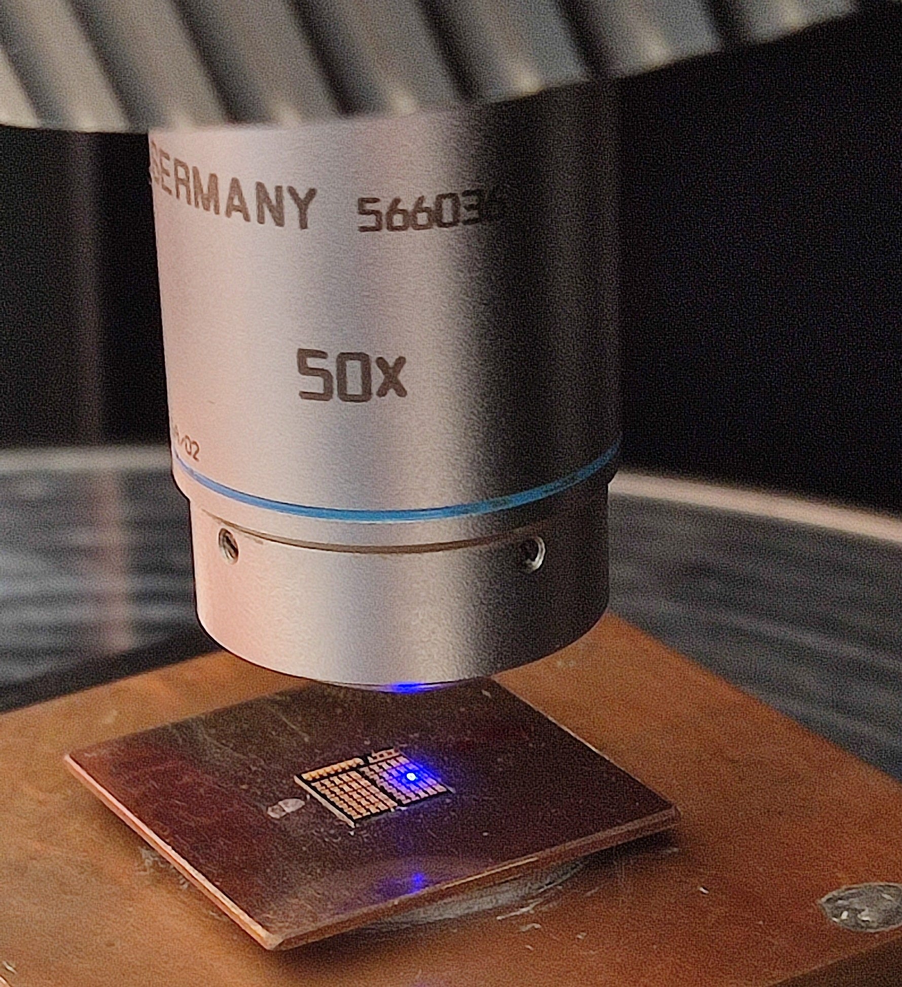
The company's technology, based on the thermoreflectance principle, which Simon prefers to call laser-based measurement, addresses the issue of measuring thermal properties. "To predict how hot a chip or device or module will get during operation, one needs to know these properties very accurately," Simon said.
These thermal properties include thermal conductivity and resistance, which describe how materials and interfaces conduct heat. If these properties are not known accurately, it is difficult to predict the peak junction temperature, which can lead to lower performance, damage, or reduced lifespan of the chip. The accurate measurement of thermal properties is crucial for designing effective cooling and thermal management systems, ensuring consistency throughout the production process, and verifying that the materials and devices meet performance specifications.
The conventional methods for measuring thermal conductivity and thermal properties, according to Simon, often cannot effectively separate multiple layers or interfaces. These methods, such as laser flash and transient plane source techniques, have been around for over 50 years. However, they typically measure bulk materials and have severe limitations when it comes to differentiating between the thermal properties of individual layers within a multi-layered structure. They also require sample processing, for instance, the samples be machined to a specific size and thickness before measurement. Thermap Solutions' laser-based instruments do not have these drawbacks.
"What we can do is optical, so we just shine laser beams onto the sample and we look at what's reflected, and that allows in situ measurement," Simon explained. "So for instance, we can measure the thermal resistance in a chip without having to do anything with it." This capability allows for the measurement of thermal resistance in a chip without any need for sample preparation.
Comparative techniques typically cannot do this and usually require specifically prepared samples. The laser-based technique also enables the assessment of the quality of bonding layers. Additionally, it can be used for identifying and imaging defects such as bubbles or voids in bonding layers or substrates. While X-ray and ultrasound techniques can also identify defects, they cannot measure the thermal properties of those defective areas. TherMap’s technology can determine how critical a defect is and whether the chip can still function reliably.
Developing Products for a Variety of Industries
The company currently has two product lines. One focuses on thin films, and the other is focused on packaging and heterogeneous integration. While there are existing companies that offer thermoreflectance products focused on thin film measurement, TherMap’s patent-pending technology extends applicability to semiconductor packaging, thicker films, and buried layers, which offers several advantages over competing techniques. The company is working to continuously innovate and maintain its competitive edge.
TherMap Solutions has partnered with Quantum Focus Instruments, a US company that manufactures advanced infrared failure analysis microscope systems and temperature measurement microscope systems for the semiconductor industry. Simon said TherMap is also starting a collaboration with the CNR IMM research laboratory in Sicily, Italy, around compound semiconductors and power electronics applications. The company also has ongoing collaborations with the University of Bristol on research projects related to heterogeneous integration and nuclear materials. Additionally, TherMap co-authored a paper with Soitec on developing the SmartSiCTM silicon carbide substrate product.
Simon sees a need for his company's products in a variety of industries.
"This is a technology that has a fairly broad application space for any materials that are layered or multi-structured," he said. Applications include the aerospace industry, where the technology can be used to measure the variable properties of fiber composites, and the battery industry, where it can be used for quality control in electrode manufacturing and cell assembly. TherMap is also working on incorporating laser ultrasonics into its system to enhance the defect imaging capabilities and is planning to combine it with other non-contact characterization techniques like electrical conductivity measurement, photoluminescence, or Raman spectroscopy.
TherMap will be looking to raise funds later this year to expand its business development and bring new products to market. The company aims to establish a stronger presence in Asia and is seeking collaborations to validate its cutting-edge measurement technology and to develop in-line versions of its instruments for integration into production lines. TherMap's primary revenue source is manufacturing instruments, and it also offers services and consultancy work.

TherMap Solutions is one of the 14 UK semiconductor startups visiting Taiwan from June 2 to 6 as part of the Global Business Innovation Programme (GBIP) led by Innovate UK. Sign up to meet Roland Simon face to face in Hsinchu:
📆 Date: Wednesday, June 4, 1:30 PM
📍 Venue: WSICC - Wei-Shun International Convention Center
📝 Registration: https://lnkd.in/gVMrmyXn
Don’t Miss Other Articles of the UK Semiconductor Startup Series:
Analogue Insight: English version ; Chinese version
Apitronix: English version ; Chinese version
TherMap Solutions: English version; Chinese version