


Takeaways from 3D IC/CoWoS for AI Summit at SEMICON Taiwan 2024
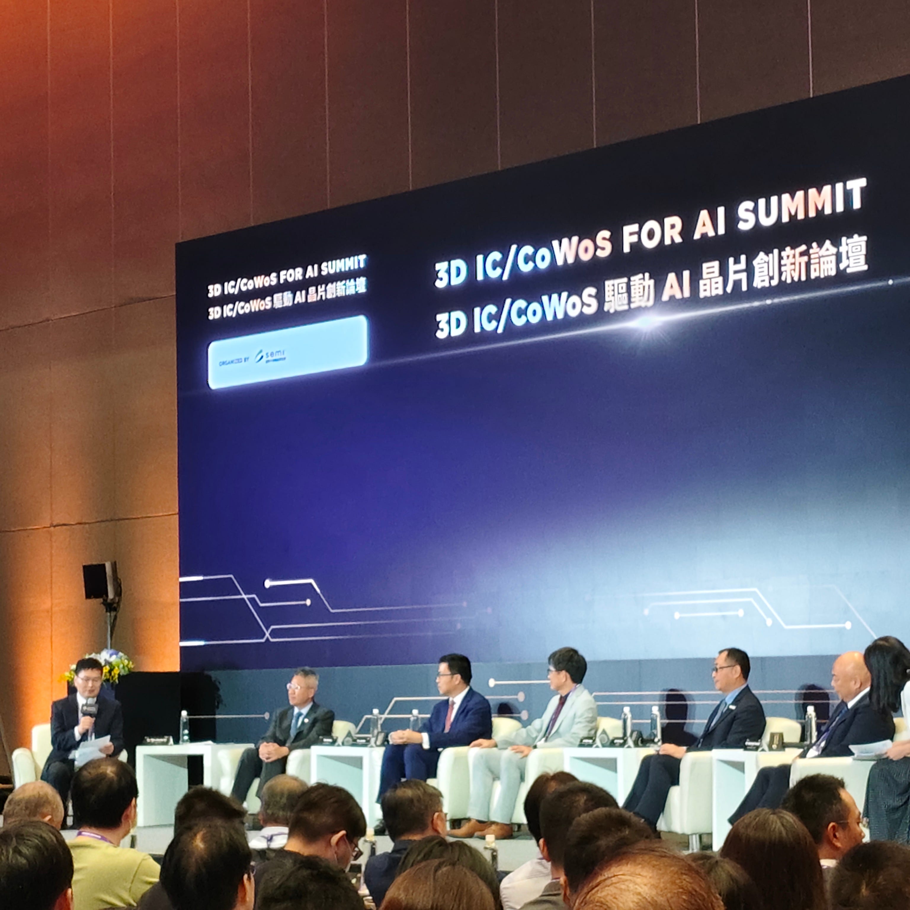
Who are the panelists?
Dr Jun He, VP, TSMC Advanced Packaging Technology and Service
Dr. Mike Hung, SVP, Quality Assurance &SiP, ASE
D. J. Lee, COO Zhen Ding Tech Group
Eric Lee, President, Scientech Corp.
Kazutoshi Horiuchi, SVP, Shubaura Mechatronics Corp
Key Takeaways from the panel
Chiplets and Stacking - One of the challenges is thermal because the density is getting higher and higher, how to dissipate the heat? The material plays a critical role.
Substrate and underfill are very important. Among those materials, you cannot only depend on Tin to solve the problem. We must make significant efforts on the interface.
The thermal material for advanced packaging is a little bit of a dual personality -the connectivity has to be good, and the thermal coupling has to be good, but the mechanical coupling can't be too good, otherwise, the stress will be too high.
It's hard to find this kind of material, so it's a good research problem for academia and the industry. We need to achieve co-optimization for the process with the support of all supply chain partners.
The semiconductor industry started mass-producing 2.5D packaging in 2013. Over the past 10 years, companies have been learning by doing. In retrospect, had we paid more attention to the development of the equipment, different systems, or the materials, the sizes, the design rules, etc, at the beginning, we would have done much better than we are doing now.
Standardization of Fan-Out PLP panel sizes and the alignment of heterogeneous integration process roadmaps are critical to everyone in the ecosystem.
The panel is a future direction, but standardization is very important for process automation.
Chiplet stacking will get more and more layers while the size of the chips is getting bigger and bigger. The shape changes from a circle to a square. However, the yield of the substrates is critical to the new processes.
Warpage is the greatest challenge for Fan-out Panel-Level-Packaging. Thanks to close collaboration with major equipment suppliers, ASE has the largest overcome this challenge, with only 6-7 mm warpage per 600x600 panel, according to Mike Hung.
The alliance also has to achieve substrate traceability, material traceability, and equipment traceability by managing machine-learning data, to achieve the best yields said Zhen Ding COO.
At the communication end of the spectrum is the AI cell phone, AIPC, AIoT, and all the many and varied applications of AI. All of these scenarios require advanced packaging - Chip-on-Wafer-on-Substrate (CoWoS) processes.
Equipment suppliers see challenges in ESD, and said photonic debunk will be an important trend for the future. Temperature detection will also be very important for 3D IC processes.
Some Taiwanese manufacturers are now making what they call Balance Fit or Anti-warpage fit that basically just sticks on the bottom of the glass substrate and reduces the warpage from greater than 10mm to smaller than 1mm.
2024 is just the beginning for AI. We have lots of work to do.