


Russia Aims to Achieve 70% of Semicon Equipment & Material Localization by 2030
According to Russian media outlet CNews, the Russian government has allocated over 240 billion rubles (approximately $2.54 billion) to support the research and development of domestic semiconductor manufacturing equipment, tools, and raw materials. The initiative aims to achieve a 70% localization of foreign semiconductor equipment and materials by 2030.
The program includes the launch of 110 R&D projects aimed at reducing reliance on imported semiconductor manufacturing equipment, with a focus on developing chips using the 28nm process. However, given the vast and complex nature of the semiconductor industry, the $2.54 billion budget is widely viewed as insufficient.
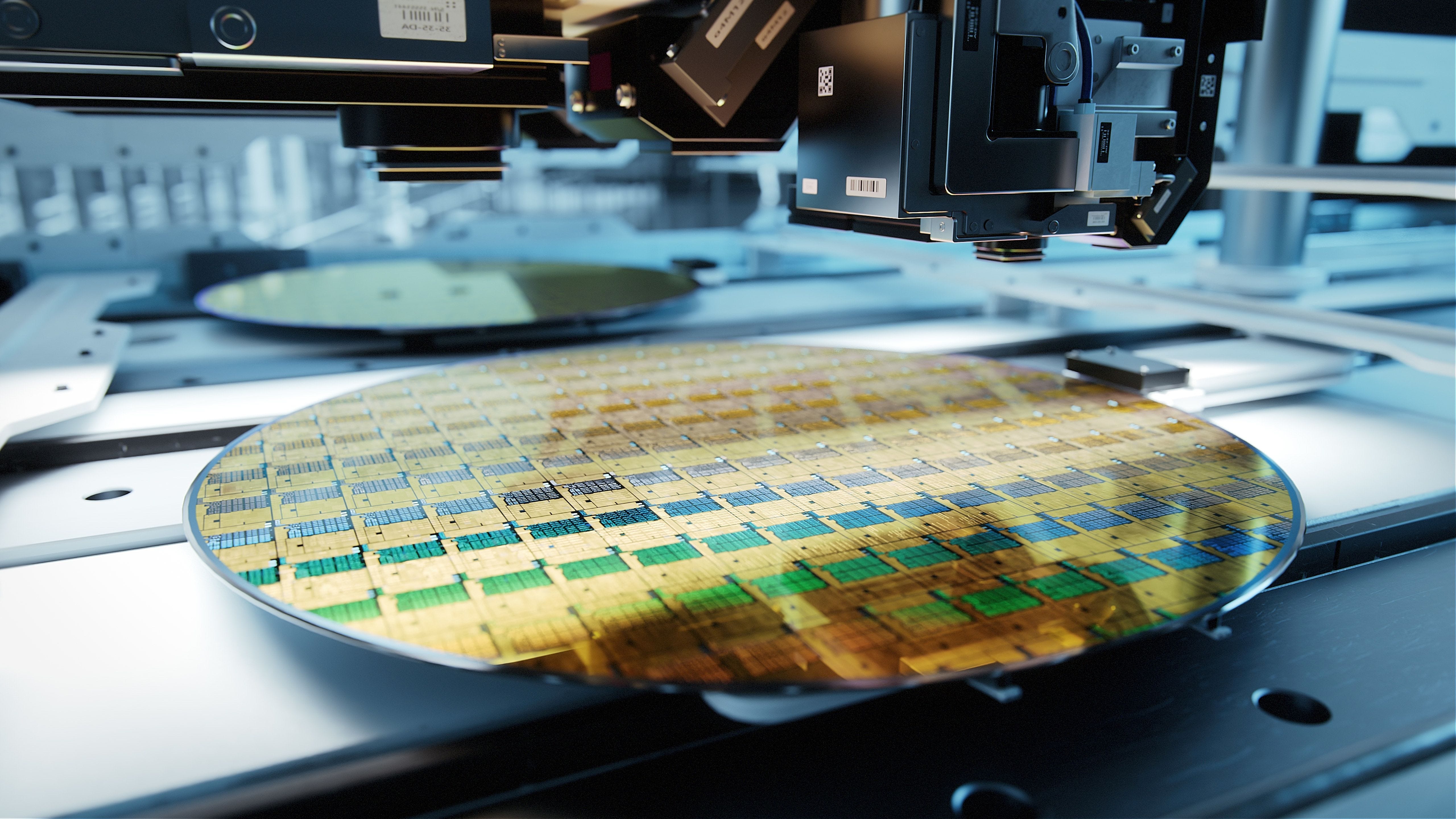
Currently, Russian chip manufacturers like Angstrem and Mikron are still producing chips at mature nodes such as 65nm and 90nm, while heavily relying on foreign equipment, particularly for photolithography. Statistics show that only 12% of the approximately 400 types of equipment required for semiconductor production in Russia can be sourced domestically.
Since the start of the Russia-Ukraine conflict in February 2022, export controls imposed by the U.S., EU, Japan, South Korea, Taiwan, and others have further complicated Russia's ability to import both chips and semiconductor manufacturing equipment. These restrictions have increased the cost of obtaining critical equipment by 40-50%, as they must often be smuggled into the country.
In response, Russia’s Ministry of Industry and Trade (Minpromtorg) and MIET, a state-owned company, have developed a program focused on developing domestic alternatives for 70% of the equipment and raw materials required for microelectronics production. This initiative spans the entire semiconductor supply chain, from equipment and raw materials to electronic design automation (EDA) tools.
The program includes the development of 20 technology routes, covering areas such as microelectronics, microwave electronics, photonics, and power electronics, with process nodes ranging from 180nm to 28nm. Some of the technologies will also be used for photomask production and electronic module assembly.
While the program's overarching goal—achieving 70% localization by 2030—is clear, many specifics remain unclear. One key milestone, expected by the end of 2026, is the completion of lithography equipment for 350nm and 130nm processes, as well as electron beam lithography equipment for 150nm nodes. Russia also plans to develop epitaxial process technology using chemical vapor deposition (CVD) equipment. Additionally, by the end of 2026, Russia aims to produce silicon ingots and wafers domestically.
By 2030, Russia hopes to independently manufacture 65nm and 90nm process wafers using domestic lithography systems, which would significantly advance its microelectronics capabilities. However, this goal still leaves Russia trailing global industry leaders by 25-28 years.
Notably, during the CIPR 2024 conference in May, Russia’s Deputy Minister of Industry and Trade, Vasily Shpak, announced that the country’s first domestically produced photolithography machine, capable of producing 350nm chips, had been completed and was undergoing testing in Zelenograd.