


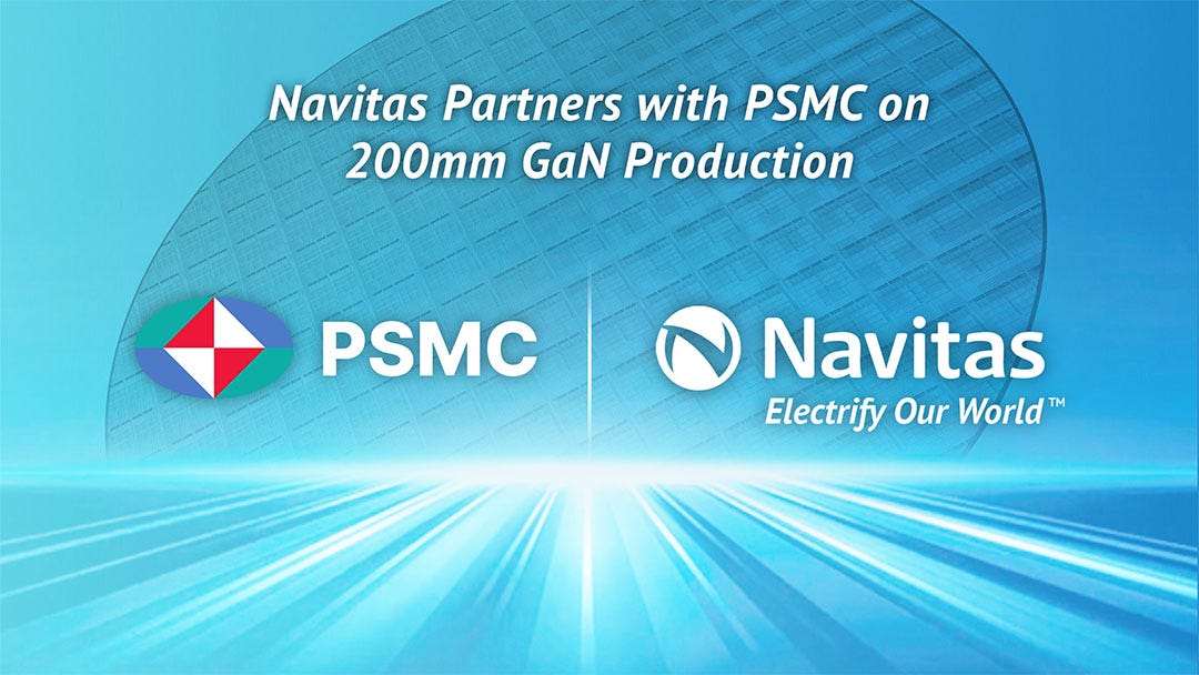
Navitas Semiconductor, a key player in GaN and silicon carbide power semiconductors, has announced a new collaboration with Power Chip Semiconductor Manufacturing Corporation (PSMC) for high-volume 200-millimeter GaN-on-silicon production. This move comes as their current partner, TSMC, is strategically exiting the GaN business. This episode aims to take a deep dive into the changing market landscape and get an understanding of future trends.
Navitas and PSMC: A Strategic Alliance for Scaled GaN Production
Navitas's partnership with PSMC aims to significantly strengthen its supply chain, drive innovation, and improve cost efficiency as GaN scales up. This alliance is specifically designed to support GaN's rapid adoption in demanding sectors such as AI, data centers, electric vehicles (EVs), solar energy, and home appliances.
PSMC will manufacture Navitas's GaN IC portfolio, ranging from 100 volts (for fast chargers) to 650 volts (for higher power applications), at their Fab 8B in Xunlian Science Park, Taiwan. This facility, operational since 2019, is capable of high-volume manufacturing for various GaN applications, including micro LEDs and RF GaN devices. A crucial advantage PSMC brings is an improved 180-nanometer CMOS process, enabling smaller, more precise circuits, leading to better performance, power efficiency, increased integration, lower costs, and improved manufacturing yields.
The transition plan involves qualification of the first devices from PSMC in Q4 2025. Navitas expects to begin volume production of its 100-volt GaN family at PSMC in the first half of 2026, with higher-power 650-volt devices transitioning from TSMC over the subsequent 12 to 24 months.
TSMC's Strategic Exit and Infineon's 300mm Push
TSMC's decision to gradually exit the GaN business entirely within the next two years is based on "market considerations and their long-term business strategy". This strategic pivot allows TSMC to double down on advanced logic manufacturing for high-margin areas like AI, high-performance computing, and smartphones, where demand is insatiable.
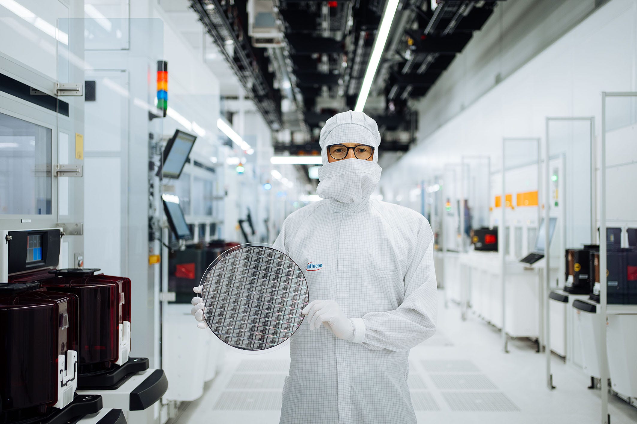
In contrast, Infineon Technologies is solidifying its position as a leading Integrated Device Manufacturer (IDM) in the GaN market by advancing its scalable GaN manufacturing on 300-millimeter wafers. Infineon's IDM model, which involves owning the entire semiconductor production process, provides advantages like high quality, faster time-to-market, and design flexibility. The company's in-house manufacturing strategy is a key differentiator. Infineon’s samples are expected by Q4 2025.
Infineon has become the first semiconductor manufacturer to successfully develop 300-millimeter GaN power wafer technology within its existing high-volume manufacturing infrastructure. This is a significant development as 300-millimeter wafers allow for the production of 2.3 times more chips per wafer compared to established 200-millimeter wafers, leading to increased efficiency. This capability, combined with Infineon's GaN expertise and broad IP portfolio, is crucial as GaN power semiconductors see rapid adoption in industrial, automotive, consumer, and computing & communication applications, including power supplies for AI systems, solar inverters, and chargers.
The Growing GaN Market and Its Applications
The global GaN semiconductor market is experiencing robust growth, valued at approximately $832 million in 2024 and projected to reach over $3.1 billion by 2032, representing a compound annual growth rate (CAGR) of about 18.18% from 2025 to 2032, according to Global Information Inc.. This growth rate is significantly higher than the overall semiconductor market. Market analysts expect GaN revenue for power applications to grow by 36% annually to approximately $2.5 billion by 2030.
GaN is considered a "wide band gap" semiconductor material, offering superior performance compared to traditional silicon. It can handle much higher voltages and temperatures, switch incredibly fast, and loses far less energy as wasted heat. This translates to devices that are not only more powerful and efficient but also dramatically smaller and lighter, as they require less bulky heat dissipation components.
Key drivers fueling this expansion include:
Surging Investments: Both private and public funding are pouring into the GaN market. For example, Cambridge GaN Devices recently closed a $32 million Series C funding round, and GlobalFoundries received $35 million in federal funding from the U.S. government in 2023 to accelerate GaN-on-silicon manufacturing.
Demand for Faster, More Efficient Charging: GaN-based chargers offer superior performance and efficiency, enabling faster charging for consumer electronics like phones, watches, and earbuds, while being significantly smaller.
Electric Vehicles (EVs): GaN power devices are increasingly integrated into core EV systems, including powertrains, onboard chargers, and inverters. This fundamentally improves energy efficiency, leading to more miles per charge and reduced charging times. For instance, Navitas has announced that Chang'an Automobile in China is using their GaNSense technology for commercial GaN-based onboard chargers.
AI and Data Centers: The immense energy demands of cloud computing, machine learning, and big data necessitate faster, more efficient power management. GaN devices enable higher power density and faster switching speeds, resulting in less wasted energy, reduced heat generation, and lower electricity bills. Navitas is collaborating with Nvidia to support GaN and silicon carbide for advanced 800-volt DC architectures in data centers.
Renewable Energy: GaN is being leveraged in solar inverters and wind power systems to dramatically enhance efficiency. GaN-based inverters can achieve power conversion efficiencies over 98%, minimizing energy loss when converting power from solar panels to the grid. Enphase, a major player in solar microinverters, is incorporating Navitas's 650V GaNFast ICs into its next-generation IQ9 system.
Challenges and the Path to Ubiquity
Despite the clear advantages and diverse applications, the high investment and manufacturing costs remain a significant restraint for widespread GaN adoption. GaN devices require more expensive raw materials (gallium and nitrogen) compared to silicon, and their manufacturing processes are more complex. A basic two-inch GaN wafer can cost between $1,900 and $2,500, a massive difference compared to a silicon wafer of the same size, which might cost only $25 to $50. GaN-on-silicon carbide wafers, preferred for high-power applications like 5G base stations, can be even more expensive, up to $3,000 per two-inch wafer.
The industry is actively working to overcome this cost barrier by scaling production, moving to larger wafers like Navitas's shift to 200-millimeter with PSMC, and refining manufacturing processes to improve yields and reduce costs. This is essential for GaN to move beyond premium applications and into the mainstream.
The strategic shifts by companies like Navitas and Infineon highlight a dynamic and rapidly evolving GaN market. While cost remains a hurdle, the relentless pursuit of energy efficiency driven by GaN is poised to redefine power electronics, leading to smaller, more efficient, and more responsive devices that will profoundly impact various aspects of our daily lives.
Identified GaN Manufacturing Sites/Foundries Worldwide:
There are 20 distinct manufacturing sites around the world that are explicitly identified in the sources as producing or being capable of producing GaN semiconductors. It's important to note that the Wikipedia list indicates it "needs to be updated" as of March 2025, so this list might not be exhaustive of all current global GaN production.
These sites include:
North America (United States):
BAE Systems in Nashua, New Hampshire, is producing GaN-on-SiC.
Qorvo in Greensboro, North Carolina, produces GaN.
Qorvo in Richardson, Texas, is producing GaN-on-SiC.
NXP Semiconductors in Chandler, Arizona, produces GaN-on-SiC pHEMT.
GlobalFoundries in Essex Junction, Vermont, is producing GaN, supported by US federal funding.
Wolfspeed in Durham, North Carolina, produces compound semiconductors and LEDs, including GaNHEMT RF ICs.
Wolfspeed in Research Triangle Park, North Carolina, producing GaNHEMT RF ICs.
Texas Instruments in Dallas, Texas, with existing GaN manufacturing.
Asia-Pacific (Taiwan & Japan):
Win Semiconductor in Taoyuan City, Taiwan, produces GaN.
Powerchip Semiconductor Manufacturing Corporation (PSMC) in Zhunan Science Park, Taiwan, has partnered with Navitas Semiconductor to begin production of 200mm GaN-on-silicon technology.
TSMC in Hsinchu, Taiwan (specifically Fab 5), has been a supplier for Navitas's 650V devices. However, TSMC has announced its decision to gradually exit the GaN business within the next two years, based on market considerations and a focus on high-growth markets like advanced processes and packaging.
Texas Instruments in Aizu, Japan, has begun production of GaN-based power semiconductors.
Vanguard International Semiconductor Corp. produces 200-mm GaN with QST transistor technologies in Hsinchu, Taiwan.
Europe (UK, Germany, Austria, Russia):
Nexperia in Stockport, England, UK, producing GaN FETs.
CSTG in Glasgow, Scotland, UK, producing GaN.
X-Fab in Dresden, Saxony, Germany, is producing GaN-on-Si.
United Monolithic Semiconductors in Ulm, Baden-Württemberg, Germany, produces GaN HEMT.
Infineon Technologies in Villach, Carinthia, Austria, produces GaN.
Syntez Microelectronics in Voronezh Oblast, Russia, produces GaN.
GaN Foundries/Manufacturing Sites in China:
Sanan IC in Xiamen, China, which operates a foundry producing GaN.
Sanan IC in Changsha, China, which also operates a foundry producing GaN, SiC, and Power devices.


Share this post