
Industry Spotlight: Navigating HBM Controls, Base Die Innovation, and Future AI Integration
Semi Vision, a research startup that cooperates with TechSoda provides the preview for its report on HBM (High Bandwidth Memory) under the context of U.S.-China export restrictions.
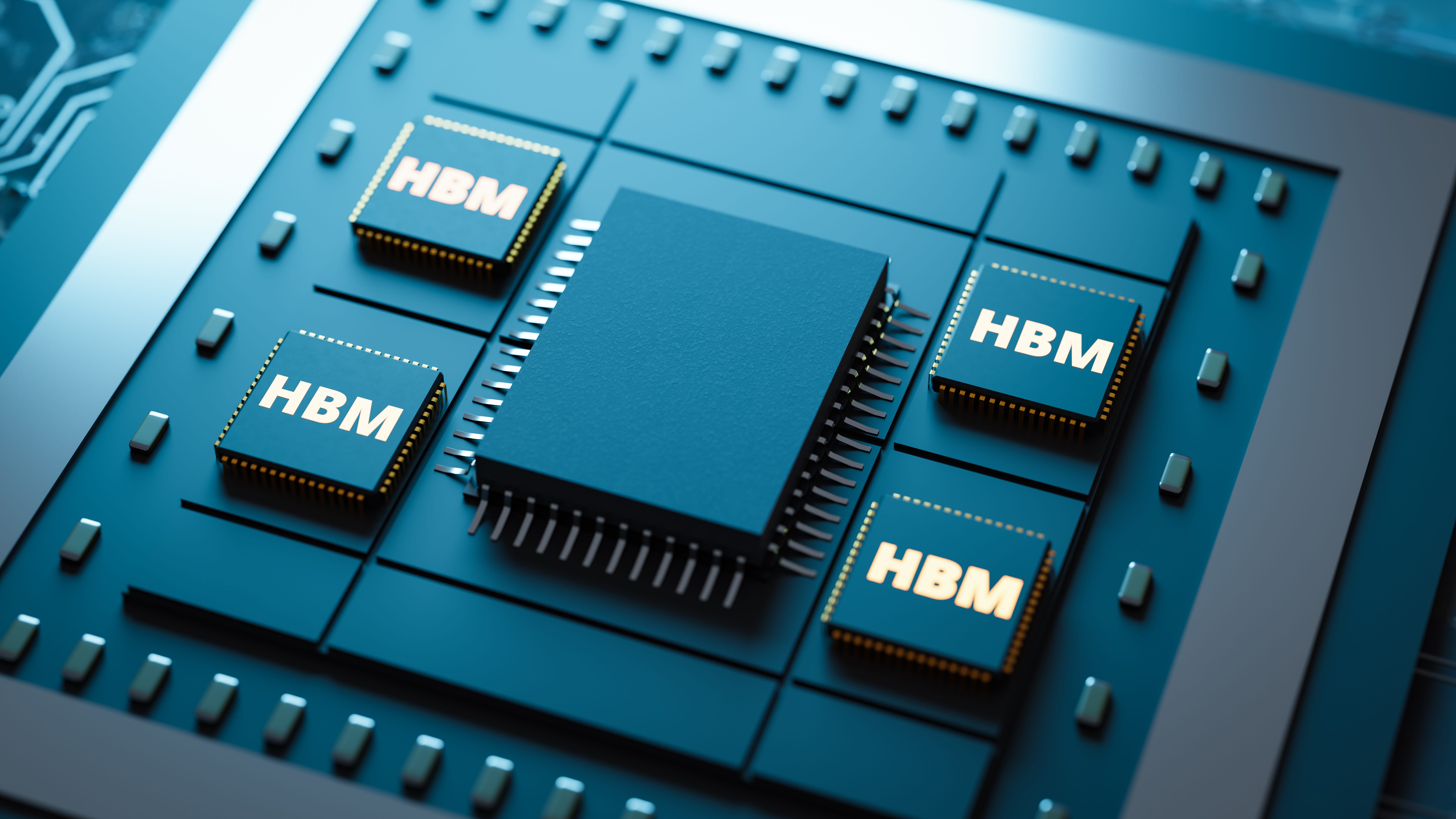
The US Bureau of Industry and Security (BIS) has introduced a significant update to its export controls, underscoring the critical importance of High Bandwidth Memory (HBM) in advanced semiconductor technologies. Under the new Export Control Classification Number (ECCN) 3A090.c, HBM stacks with a ‘memory bandwidth density’ exceeding 2GB per second per square millimeter (mm) will now be controlled. Notably, this threshold applies to all HBM stacks currently in production.
What’s Changing and Why It Matters
To maintain the efficacy of these controls, BIS has adopted bandwidth density rather than overall bandwidth as the defining metric. This approach ensures that controls remain applicable even as manufacturers scale performance by integrating more HBM chips without significantly increasing cost.
While the 3A090.c technical note excludes certain co-packaged ICs with HBM and logic — where the IC’s primary function is processing — it clarifies that HBM permanently affixed to a logic IC with a control interface and PHY (Physical Layer) function remains within scope. This brings the design of the HBM base die into sharp focus, an area that represents the intersection of materials, equipment, advanced packaging, and specialized IP.
Deep Dive: The HBM Supply Chain Under the Microscope
Semi Vision’s upcoming analysis will provide a comprehensive look at the following critical areas of the HBM supply chain:
Silicon Wafer: The foundational layer for HBM manufacturing.
Molding Process: Ensuring structural integrity and alignment.
Thermo-Compression Bonding (TCB): Precision techniques for efficient interconnectivity.
Hybrid Bonding: Next-generation bonding technology enhancing packaging density.
Dicing/Grinding: Processes that impact yield and HBM performance.
Chemical Mechanical Polishing (CMP): Critical for achieving ultra-flat surfaces.
HBM IP: Enabling advanced design and seamless integration.
Notable Industry Developments
TSMC has already adopted advanced 12nm and 5nm logic technologies for HBM applications, setting a new standard for integration.
Companies like Marvell and Broadcom are pioneering custom HBM solutions through their advanced packaging platforms.
Future iterations of HBM technology are rapidly evolving: HBM3E will soon transition to HBM4, introducing further advancements, while HBM5 is expected to leverage innovative 3D System-in-Package (SiP) concepts.
Future Focus: AI and Beyond
The AI industry’s insatiable demand for higher performance and efficiency puts HBM advancements at the forefront of innovation. Semi Vision’s report will pay particular attention to two pivotal areas that will shape the next decade of AI hardware:
HBM Advancements – Continued innovation in bandwidth, density, and integration.
Silicon Photonics Integration – Addressing energy efficiency and scaling challenges for AI workloads.
From regulatory impacts to supply chain intricacies and next-gen innovations, Semi Vision’s analysis will equip industry stakeholders with actionable insights to navigate the evolving HBM landscape.
Stay ahead of the curve as we explore the intersection of HBM design, advanced packaging, and AI hardware integration.
Follow Semi Vision’s substack for the upcoming reports, analysis, and expert commentary. Consulting services will be available in January 2025.