
Huawei Discloses Mass-Production Test Data and Roadmaps in "Tau Law V2" Paper
TSMC and Intel maintain a significant, multi-generation logic leadership lead, but China is surely steadily progressing.
He Tingbo, head of Huawei’s Semiconductor Unit, has released the paper “Time Miniaturization Theory for Multi-Tier Electronic Systems” —also known in the industry as the Tau Law Version 2— on Chinaxiv, the Chinese Academy of Sciences’ Preprint platform. The engineering and theoretical paper expands on the V1 framework introduced in May, adding mass-production test data, architectural specifications, and an explicit multi-generation roadmap for the company’s Kirin processor lineup.
As traditional physical scaling faces increasing lithography and equipment constraints, the paper details an alternative architectural approach that uses the time constant, rather than transistor area, as its primary metric of development.
Technical Framework: Mechanics of the Tau Law and LogicFolding
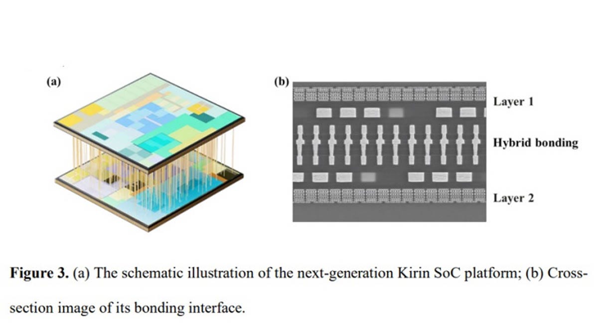
Huawei’s Tau Law proposal focuses on optimizing time scaling rather than reducing physical area. Alongside this approach, the paper outlines a 3D design architecture named LogicFolding, which distributes digital, analog, and memory circuits across stacked tiers.
According to the documentation, when the hybrid bonding pitch matches the top-layer metal wiring dimensions, design optimization shifts from macro-block divisions to cell-level constant optimization. This method enables optical logic partitioning, bypassing standard 3D stacking limitations that traditionally restrict vertical layers to distinct functional blocks.
Huawei claims that at a fixed device node, the LogicFolding architecture can deliver a 55% step-wise increase in transistor density and a 41% improvement in power efficiency.
Measured Gains: Kirin 2026 vs. Kirin 9030 Pro
The V2 paper includes comparative mass-production test data evaluating the upcoming Kirin 2026 mobile SoC against the current flagship Kirin 9030 Pro (a planar, 9-core, 14-thread platform with an ultra-large core clocked at 2.75 GHz).
When tested at an identical performance output and a controlled ambient temperature of 25°C, the upcoming 3D-stacked processor shows notable reductions in operating voltage and overall physical footprint:
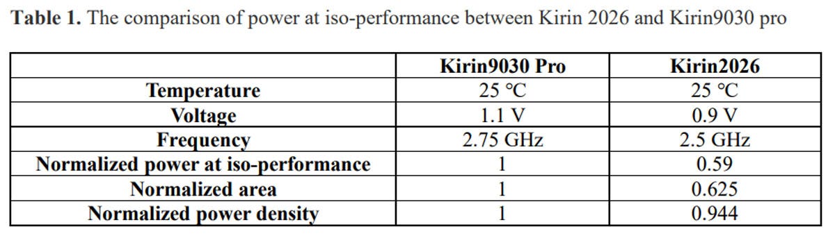
By dropping the core operating voltage from 1.1V to 0.9V, the design curtails transistor switching losses. Additionally, reducing the core die area to 62.5% of the previous generation allows for tighter structural integration within mobile devices—potentially freeing up space for batteries or other internal modules—while lowering per-wafer manufacturing thresholds.
Frequency Roadmaps and Development Status
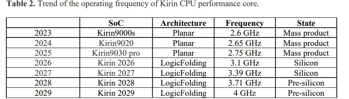
The Tau Law V2 paper publicly details a multi-year roadmap spanning four subsequent generations of Kirin silicon, targeting steady frequency increases for its CPU performance cores:
Kirin 2026: Clocks in at 3.1 GHz. This represents a 0.35 GHz single-generation increase over the Kirin 9030 Pro, following a period where cumulative frequency gains across the prior three generations totaled 0.15 GHz.
Kirin 2027: Projected at 3.39 GHz.
Kirin 2028: Projected at 3.71 GHz.
Kirin 2029: Targets a frequency of 4.0 GHz.
Current Silicon Development Status
The paper provides specific markers regarding the physical progression of these designs through the hardware pipeline:
The Kirin 2026 and Kirin 2027 models have completed their initial tape-outs and are currently in the silicon validation and hardware testing phase. The Kirin 2026 is scheduled for a commercial debut this fall, slated to power the upcoming Mate 90 smartphone series.
The Kirin 2028 and Kirin 2029 iterations have finalized their front-end architecture designs and are navigating final design verification stages before physical tape-out.
Industry Context: Huawei’s Tau Law and LogicFolding architectures represent a clear effort to maximize the performance of existing, accessible process nodes through advanced packaging and alternative design mathematics. While the published data outlines substantial theoretical and lab-tested efficiency gains, the true efficacy of this approach will be determined when the Kirin 2026 faces real-world performance workloads and commercial mass-production yields this fall.
When independent research labs (like SemiAnalysis) tore down the Kirin 9030 Pro, they confirmed it was built on SMIC’s N+3 process, which is an advanced 7nm-class (or roughly 6nm-class) node squeezed to its absolute limit using older DUV lithography without EUV machines.
For the upcoming Kirin 2026, Huawei is using “LogicFolding” (3D vertical chip stacking) to stack multiple layers of that 7nm-class silicon on top of each other.
Huawei has laid out an ambitious roadmap: starting from the Kirin 9030’s big-core frequency of 2.75GHz, lab samples have already hit 3.39GHz, with a target of 4GHz by 2029. It also aims to push equivalent transistor density to 295 MTr/mm², putting it on par with TSMC’s 14A node, according to SemiAnalysis. The same report also revealed that the Kirin 9030 Pro chip provides 10% higher transistor density than Intel Panther Lake CPUs, which are produced by Intel's 18A process. This implies that SMIC is gradually inching towards 3-5nm chip process technology.
SemiAnalysis is cautious about these claims, noting that Huawei calculates density differently from traditional foundries — measuring 3D-stacked chips based on total packaging area, which inflates the numbers when multiple active logic layers are stacked. Applying the same method to AMD’s MI450X (which combines an N2 top layer with an N3P bottom layer) would yield a theoretical density of 460.2 MTr/mm², well beyond Huawei’s 2031 target.
It is now clear that Huawei is effectively bypassing EUV by shifting “foundry-level” work onto system designers to work around process limitations. A report by O’Daily pointed out that while AMD already uses 3D stacking (e.g., V-Cache for cache memory, and moving I/O/interconnect to the base die in MI350X), Huawei’s approach goes further — splitting a single logic block itself and distributing it across vertical layers, which poses a far greater engineering challenge.
Dr. B.W. Yang, Jointly Appointed Professor of National Tsing Hua University, explains:
Huawei’s "LogicFolding" architecture represents a strategic departure from traditional semiconductor development, leveraging "hybrid bonding" technology to achieve performance gains without relying on advanced Extreme Ultraviolet (EUV) lithography. This approach aligns and fuses signal contact points on two wafers, significantly expanding signal connectivity—for a 4-square-centimeter chip, the number of signal connection points increases from approximately 12,000 to over 1 million.
The Strategic Pivot: Bypassing Lithography Constraints.
To circumvent U.S. technology export controls, Huawei has prioritized Wafer-to-Wafer (W2W) hybrid bonding over Die-to-Wafer (D2W) technology. While D2W equipment is subject to strict export controls from the U.S., the Netherlands, and Japan, W2W equipment—championed by Austria's EVG Group—remains more accessible. Furthermore, Huawei has hedged against future restrictions through China’s “Big Fund Phase III,” which has enabled domestic equipment makers like Naura and Piotech to supply hybrid bonding packaging tools that support the necessary 1.5-micron pitch LogicFolding and the Tau (τ) Law.
Huawei’s broader framework for this strategy is the "Tau Law" (τ), which shifts the primary metric of semiconductor progress from geometric scaling (shrinking transistors, as in Moore’s Law) to "time scaling." By focusing on reducing the resistive-capacitive load and propagation delay—the time it takes for an electrical signal to travel through a circuit—Huawei aims to optimize performance through architecture rather than raw lithography. LogicFolding is the physical manifestation of this theory.
This approach mirrors the innovation strategy seen in firms like DeepSeek: constrained by the inability to access frontier hardware (such as advanced GPUs or EUV lithography), the company has been forced to innovate in system architecture to maintain competitiveness. If Huawei successfully generalizes LogicFolding from two-layer to multi-layer dies, the Tau Law could fundamentally alter the long-term roadmap for high-performance computing (HPC) and AI system integration, proving that advanced packaging can serve as a viable alternative pathway for silicon sovereignty.
