
De-Risking Next-Gen Semiconductor Innovation and Building North America’s Secure Defense Hub in Edmonton, Canada
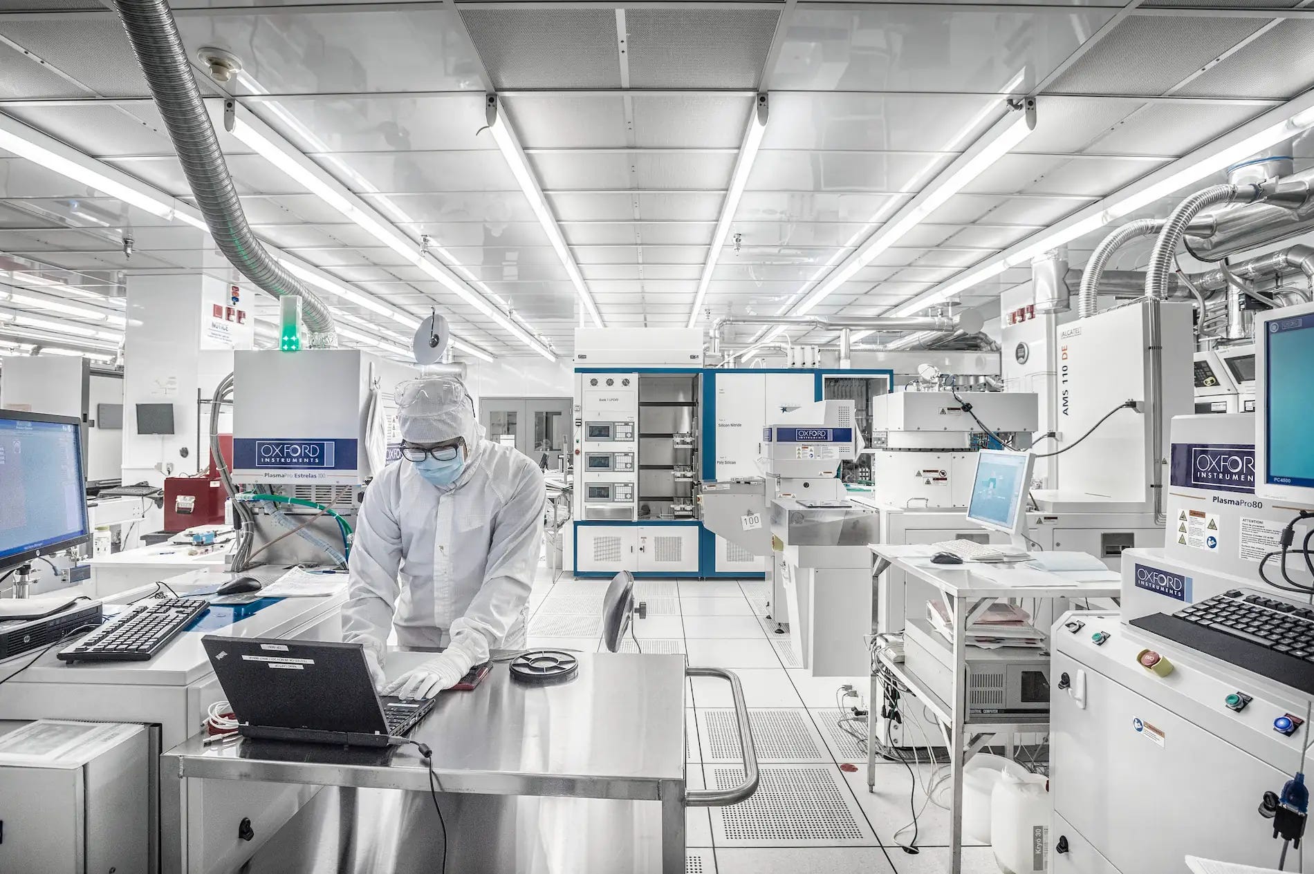
As the global semiconductor industry grapples with capacity bottlenecks, soaring capital expenses, and escalating geopolitical tensions, an unexpected player is emerging as a critical node in the global tech supply chain. Edmonton, Alberta—long celebrated as a bedrock for energy and industrial manufacturing—is rapidly positioning itself as an agile, low-barrier haven for advanced research, development, and secure hardware prototyping.
In an exclusive interview, Dr. Eric Flaim, Director of the University of Alberta’s nanoFAB, and Brent Jensen, Senior Director of Edmonton Global, detailed how the region is uniquely equipped to de-risk high-volume manufacturing for international tech giants, specifically targeting pioneering fields like quantum computing, photonics, and sovereign defense technologies.
Agile Prototyping and Quantum Capabilities
For major semiconductor foundries and fabless designers, securing facility time for experimental architecture or low-volume runs is notoriously difficult. Major fabs operate on rigid, high-volume repetition where deviations can disrupt multi-billion dollar schedules.
“Where we feel our value proposition has been... is really in our highly flexible, low-barrier, cost-effective approach to prototyping and small-volume manufacturing,” says Dr. Flaim. Operating under an open-access model backed by a dedicated technical staff, nanoFAB allows companies to test non-standard materials and iterative designs without capital exposure.
A major technical differentiator for the facility is its integrated, correlative workflow. Within a single administrative structure, developers can transition instantly from multi-material deposition and specialized etching (working with advanced materials like barium titanate, lithium niobate, and III-V materials) directly into high-end transmission electron microscopes (TEM) and atomic-scale spectroscopy. This allows designers to analyze structural interfaces immediately and diagnose failures in real time.
Specializing in the Quantum and Photonic Frontiers
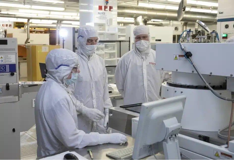
As Taiwanese IC designers and research entities push past standard silicon constraints into heterogeneous integration, 3D IC stacking, and specialized chips, nanoFAB provides a dedicated launchpad.
The facility is specifically equipped for:
Photonic Quantum Systems: Processing advanced optical and photonic device designs.
Superconducting Qubit Systems: Manufacturing device architectures for quantum computing qubits.
Currently operating on a 6-inch (150 mm) wafer line, the facility is gearing up for the future. Backed by a recently secured $20 million provincial investment, nanoFAB is initiating the build-out of an 8-inch (200 mm) wafer line to meet evolving industrial scales. Through a co-location model, nanoFAB is inviting global partners to relocate or invest in equipment within their cleanrooms, removing the operational burden of maintenance and technician overhead from private enterprises.
A Sovereign Stronghold: Developing Edmonton’s Secure Defense Hub
Beyond commercial prototyping, the Canadian federal government’s strategic mandate to boost defense spending amid global trade instability is reshaping Edmonton’s semiconductor landscape.
The region is officially establishing a secure semiconductor device fabrication center. Managed by the nanoFAB team but structurally separate from regular commercial cleanrooms, this dedicated 8-inch manufacturing line will operate within a completely sovereign, secure environment.
“There needs to be a separate type of facility catering towards that type of technology development manufacturing, especially within a sovereign and secure kind of environment,” Dr. Flaim emphasized.
The center will explicitly target dual-use and military technology developments, focusing heavily on components required for:
Next-generation radar systems.
Advanced quantum sensors.
The initial $20 million funding acts as a catalyst, with project leaders actively seeking an additional $50 million to $60 million from federal frameworks over the next 6 to 12 months. Initial components of the secure facility are slated to come online within 12 to 18 months, with heavy equipment integrations completing in the 24-to-36-month window. This infrastructure offers global technology firms a reliable pathway into Western defense supply chains.

The Edmonton Advantage: AI Integration, Clean Energy, and Soft Landings
Beyond the cleanroom walls, Edmonton Global points to a holistic ecosystem already taking shape — one purpose-built to support long-term tech scaling.
1. The Silicon-AI Synergy
As testing and process migrations slip below the 2-nanometer and angstrom thresholds, hardware design requires deep integration with Artificial Intelligence. Edmonton is globally ranked as a premier AI research powerhouse. It is home to the Alberta Machine Intelligence Institute (Amii), one of Canada’s three national AI hubs, which specializes heavily in machine learning. Through this localized ecosystem, hardware designers can collaborate directly with world-class software researchers to optimize silicon architectures, edge AI hardware, and agentic AI efficiency at the fundamental chip level.
2. Powering Sustainable Infrastructure
The massive power demands of advanced packaging and AI data centers are met by Alberta’s unique grid capabilities and clean energy pivot. Possessing a current grid buffer zone of 1.2 to 1.5 gigawatts, the region offers an incredibly competitive architecture for private tech enterprises through “behind-the-fence” power generation. Companies can utilize local natural gas pipelines coupled with world-class regional carbon capture and storage (CCS) trunklines to achieve carbon neutrality.
Furthermore, the area is an incubator for heavy-duty thermal management, featuring industry stalwarts like CoolIT Systems (advanced liquid cooling) and Silent-Aire (hyperscale data center manufacturing), alongside quantum cooling innovators like Zero Point Cryogenics.
3. Political Stability and Talent Trajectories
In a climate dictated by shifting US tariff policies and bilateral tensions, Canada represents the ultimate G7 “soft landing pad”. Boasting more comprehensive global free trade agreements than any of its G7 peers and maintaining an intensely predictable political and banking infrastructure, the region minimizes international expansion risks.
Importantly, Edmonton solves the critical talent deficit dogging other North American expansions. The city’s population has expanded by 25% over the last five years alone, driven by highly international, skilled talent pools. Working alongside the University of Alberta and the Northern Alberta Institute of Technology (NAIT), the region routinely constructs tailored, course-based Masters of Engineering programs, specialized training bootcamps, and technician pipelines designed in direct coordination with corporate partners.
R&D as the Strategic Anchor
Rather than seeking to drain global talent, Edmonton’s vision focuses on acting as a specialized, collaborative global partner. Pointing to the historical precedent of how TSMC established its footprint in Japan—beginning with an R&D and material testing center in Yokohama before scaling to major fabrication facilities in Kumamoto—Brent Jensen notes that research partnerships are the ideal starting point.
“We have the capacity and the capability right now, and we’re growing,” says Jensen. For global semiconductor enterprises seeking to de-risk their future roadmaps, Edmonton represents a stable, highly advanced environment to co-design and build the next frontier of tech hardware.
Book a meeting and meet Dr. Eric Flaim and Brent Jensen at Computex 2026!